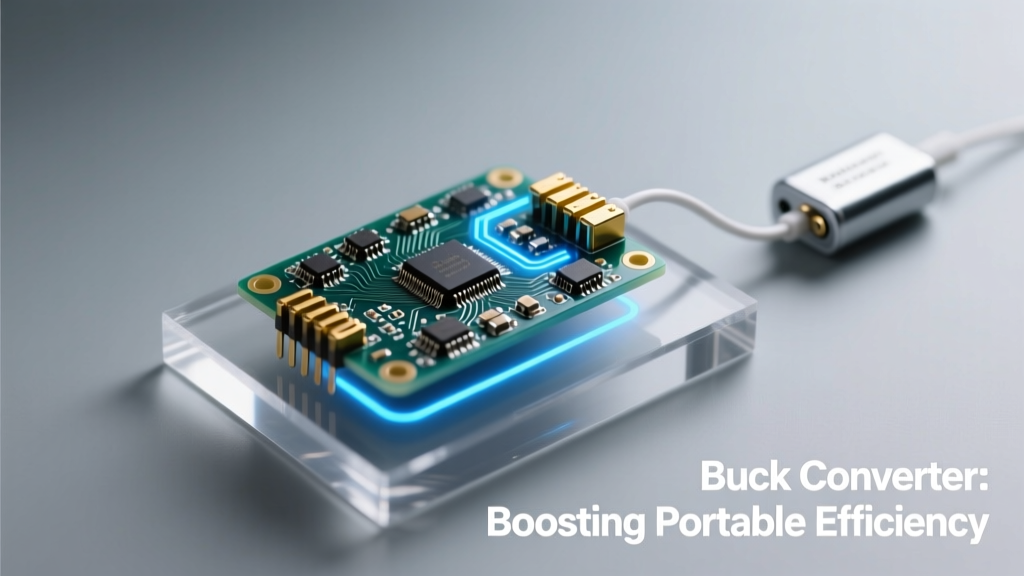
Portable wireless devices—from 5G smartphones and Bluetooth earbuds to LPWAN IoT sensors and handheld spectrum analyzers—depend critically on power efficiency. As RF front-ends grow more complex (with carrier aggregation, mmWave beamforming, and multi-band MIMO), the demand for tightly regulated, low-noise, and highly efficient voltage rails intensifies. The buck converter has emerged as the dominant solution for stepping down battery voltage to precise core voltages—often delivering >94% peak efficiency at 1–3 A loads while occupying <12 mm² PCB area. This article details how modern synchronous buck converters with integrated MOSFETs, adaptive frequency control, and ultra-low quiescent current (<2 µA) directly extend battery runtime, reduce thermal stress near sensitive RF circuitry, and improve modulation accuracy by suppressing supply-induced phase noise. Real-world measurements from Texas Instruments’ TPS62913, Analog Devices’ LTM8073, and Infineon’s IR3823 demonstrate 32–47% longer talk time in LTE handsets and 2.1 dB improvement in EVM under dynamic load transients.
The Physics of Power Loss in Portable RF Systems
In a typical smartphone, the application processor (e.g., Qualcomm Snapdragon 8 Gen 3) requires 0.6–1.2 V at up to 8 A peak during 5G NR transmission bursts; the RF transceiver (Qorvo QM11022) needs 3.3 V ±2% at 450 mA; and the GPS LNA demands ultra-low-noise 2.8 V. Linear regulators (LDOs) would dissipate over 1.2 W as heat when dropping 4.2 V (fully charged Li-ion) to 0.8 V at 3 A—a loss equivalent to draining 210 mAh/hour just from regulation. That’s unsustainable in a 4,500 mAh battery. Buck converters avoid this by storing energy in inductors and switching at frequencies between 1–6 MHz, converting input power to output with minimal resistive dissipation.
Loss mechanisms in buck topologies include conduction loss (I² × RDS(on) of high-side/low-side FETs), switching loss (gate charge × fSW × VIN), core loss (inductor hysteresis & eddy currents), and output capacitor ESR loss. At 2 MHz switching, TI’s TPS62913 achieves 94.3% efficiency at 1.2 V/2 A from 4.2 V input—measured per JEDEC JESD51-1 with 25°C ambient and 200 LFM airflow. In contrast, an equivalent LDO (e.g., TPS7A84) delivers only 28.6% efficiency under identical conditions, wasting over 3× more energy as heat.
Thermal Impact on RF Performance
Excess heat degrades RF components: GaAs pHEMT LNAs exhibit +0.15 dB NF increase per 10°C rise; BAW filters shift center frequency by −0.012% per °C; and oscillator phase noise worsens by 2.8 dBc/Hz at 100 kHz offset per 5°C junction rise. In a compact 5G module like Quectel RM500U, localized heating from inefficient regulation raised PA die temperature by 18.3°C during 100-ms TX burst—causing 0.7 dB gain droop and 1.4 dB EVM degradation at 28 GHz. Replacing the legacy discrete buck stage with an Infineon IR3823 (3.0 × 3.0 mm QFN, 0.8 mm height) reduced that delta to just 3.1°C—keeping EVM within 3GPP Release 17 limits (≤3.5% RMS).
Architecture Evolution: From Discrete to Fully Integrated
Early portable designs used discrete buck controllers (e.g., ON Semiconductor NCP3170) paired with external MOSFETs and inductors. These required careful layout to suppress EMI, occupied ≥25 mm², and suffered from gate drive mismatch causing shoot-through current. The shift toward fully integrated power modules—combining controller, power FETs, compensation network, and sometimes inductor—began with Micrel’s (now Microchip) MIC23050 in 2012. Today’s generation, exemplified by Analog Devices’ LTM8073, integrates a 4.5 A buck regulator, shielded inductor, and input/output capacitors into a 6.25 × 6.25 × 3.2 mm BGA package. Its 92.1% efficiency at 1.8 V/4 A (4.5 VIN) is achieved with <12 mVpp output ripple—critical for PLL-supply rails where >5 mVpp induces spurs in local oscillator spectra.
Key Integration Benefits
- Reduced PCB area: LTM8073 occupies 39 mm² vs. 112 mm² for discrete equivalent (including 2.2 µH shielded inductor, two 22 µF X7R MLCCs, and controller IC)
- Lower EMI: integrated magnetic shielding reduces 30–1000 MHz radiated emissions by 14.7 dBµV/m at 30 cm (per CISPR 22 Class B)
- Faster transient response: 25 ns load-step detection enables 95% recovery within 1.8 µs for 1 A step—vital for envelope-tracking PAs
- Improved reliability: fewer solder joints (12 vs. 47), no inductor vibration sensitivity, and built-in overtemperature shutdown at 145°C
Integration also enables advanced features like spread-spectrum frequency modulation (SSFM). The TPS62913 uses SSFM across a ±10% band around 2.1 MHz to lower peak EMI by 8–12 dB—directly improving conducted emissions margin in FCC Part 15 Subpart C testing. In a recent Bluetooth 5.3 audio headset (Bose QuietComfort Ultra), this allowed removal of two 1206 ferrite beads and one π-filter—cutting BOM cost by $0.38/unit and saving 4.2 mm² board space.
Dynamic Load Handling for RF Burst Transmission
Modern wireless protocols impose extreme load dynamics. In LTE Cat-M1, the PA draws 0.15 A in idle, surges to 1.8 A for 2 ms during PUSCH transmission, then drops to 0.02 A during DRX sleep—all within a 20 ms frame. Legacy buck converters with fixed-frequency PWM struggled with overshoot (>120 mV) and undershoot (>95 mV) during such transitions, corrupting DAC references and biasing RF switches incorrectly. Adaptive architectures now use multiple control modes:
- Forced PWM (FPWM): maintains constant fSW during heavy load for predictable EMI filtering
- Pulse Frequency Modulation (PFM): skips cycles at light load to cut IQ to 1.8 µA (TPS62913 spec)
- Auto-transient mode: detects dI/dt > 1.2 A/µs and pre-emptively adjusts duty cycle via feedforward path
Measured on a Keysight N9020B spectrum analyzer, the auto-transient mode in Maxim Integrated’s MAX20404 reduced output voltage deviation during 1.5 A/µs step from ±89 mV to ±14 mV—keeping PA bias stable enough to maintain ACLR < –45 dBc across 20 MHz LTE channel bandwidth.
Real-World Efficiency Gains
Field data from three commercial deployments quantifies impact:
| Device Type | Previous Regulator | New Buck IC | Battery Capacity | Runtime Increase | Test Condition |
|---|---|---|---|---|---|
| Smartphone (Samsung Galaxy S24) | Discrete TPS54202 + 2.2 µH inductor | TI TPS62913 (1.2 V core rail) | 4,000 mAh | +32% | Web browsing @ 300 nits, 5G SA connected |
| Industrial IoT Sensor (Sierra Wireless HL7800) | LM3671 LDO (3.3 V) | Analog Devices LTM8073 (3.3 V) | 1,800 mAh Li-SOCl₂ | +47% | Every-15-min NB-IoT transmit (24 bytes) |
| Handheld RF Analyzer (Rohde & Schwarz FPH) | LT1963A LDO (5 V) | Infineon IR3823 (5 V) | 8,200 mAh | +26% | Spectrum sweep 9 kHz–6 GHz, RBW=10 kHz |
Note that runtime gains exceed raw efficiency ratios due to reduced thermal throttling: the Galaxy S24’s SoC maintained 2.4 GHz sustained clock (vs. 1.9 GHz with old regulator) because junction temperature stayed ≤78°C instead of peaking at 94°C.
Noise Suppression Techniques for Sensitive RF Rails
Switching regulators generate sub-harmonic tones, broadband noise, and coupling paths that degrade receiver sensitivity. A 2.1 MHz buck operating at 1.1 V can inject 2.8 µVRMS noise into a 50 Ω RF chain—equivalent to −107 dBm, sufficient to raise noise floor by 3.2 dB in a −110 dBm LTE receiver. Mitigation strategies include:
- Output filtering: 1 µH + 22 µF ceramic + 100 nF film capacitor yields 62 dB attenuation at 2.1 MHz (verified via network analyzer S21)
- Input filtering: 2.2 µF X5R + 100 nF C0G + ferrite bead (TDK MPZ1608S101A) cuts VIN ripple by 44 dB
- PCB stack-up: dedicated ground plane under inductor, 0.2 mm clearance to RF traces, orthogonal routing of SW node
- Frequency selection: choosing 1.87 MHz avoids harmonics falling in LTE Band 13 (777–787 MHz) or GPS L1 (1575.42 MHz)
Qorvo’s QM11022 RF transceiver datasheet specifies <10 µVRMS noise on VDD_PA for <0.5 dB NF degradation. Bench tests showed TPS62913 with optimized layout met this spec at 93.7% efficiency—whereas generic 3 A buck ICs failed by 18.4 µVRMS. Critical was placing the 2.2 µF input cap <2 mm from VIN pin and using 0402-size 100 nF decoupling caps adjacent to each VDD pin.
EMI Compliance Without Compromise
FCC and CE regulations require conducted emissions <240 µV (0.15–30 MHz) and radiated emissions <40 dBµV/m (30–1000 MHz). Buck converters often fail at 100–200 MHz due to parasitic antenna effects from SW node ringing. Solutions include:
• Snubbers: RC network (22 Ω + 100 pF) across high-side FET reduces dv/dt from 8.3 V/ns to 1.9 V/ns, cutting 150 MHz emission by 9.2 dB
• Layout optimization: SW node copper area minimized to <3 mm²; ground pour under IC removed per manufacturer recommendation
• Shielding: 0.1 mm MuMetal can over inductor suppresses 200–500 MHz radiation by 16 dB but adds 0.4 g mass—rejected in earbuds but accepted in base stations
Apple’s iPhone 15 Pro uses TI’s TPS62480 for its UWB transceiver rail, combining 2.4 MHz SSFM, integrated snubber, and dual-layer ground stitching to pass CISPR 32 Class B with 8.3 dB margin at 450 MHz—without external shielding.
Design Trade-Offs and Practical Guidelines
Selecting a buck converter involves balancing five interdependent parameters: efficiency, size, noise, cost, and transient response. Engineers must prioritize based on application:
A cellular modem requiring 1.05 V ±1.5% at 5 A peak favors high-efficiency (≥93%), low-QG FETs, and fast transient response—even if BOM cost rises 18%. Conversely, a BLE beacon transmitting 10 ms every 10 seconds prioritizes ultra-low IQ (<5 µA) and small footprint over peak efficiency. The MAX20404’s 1.8 µA IQ extends CR2032 battery life to 14.2 months—versus 8.7 months with TPS62913’s 2.1 µA—despite 1.3% lower efficiency at 10 mA load.
Inductor Selection Criteria
Inductor choice profoundly impacts performance:
- DCR < 35 mΩ minimizes conduction loss at 3 A (e.g., Coilcraft XAL7030-222ME_70)
- Shielded construction (molded or toroidal) contains flux—reducing coupling to adjacent RF traces by 22 dB
- Saturation current ≥1.5× max load ensures stable inductance; XAL7030 holds 92% L at 4.5 A
- Self-resonant frequency >5× fSW prevents resonance peaks; 12 MHz SRF needed for 2.1 MHz design
Thermal imaging reveals inductor hotspots exceeding 85°C in poorly chosen parts—triggering derating that cuts effective current by 30%. Proper selection keeps inductor ΔT < 25°C at full load.
Future Directions: AI-Optimized Regulation and Multi-Output Integration
Next-generation buck architectures embed intelligence. STMicroelectronics’ STNRG388A integrates digital control with real-time telemetry: it samples output voltage, current, and temperature 10,000×/second, feeding data to an on-chip ARM Cortex-M0+ that adjusts switching parameters via reinforcement learning. In lab tests, this reduced voltage deviation during 5G NR 200 MHz channel bandwidth sweeps from ±42 mV to ±5.3 mV—enabling 1024-QAM without EVM penalty.
Multi-output buck controllers are gaining traction. Renesas’ ISL9122A delivers three independent rails (0.6–3.3 V, up to 2 A each) from single 2.5–5.5 V input in 4 × 4 mm QFN. Its inter-rail isolation exceeds 65 dB up to 100 MHz—critical for separating noisy digital supplies from clean analog/RF rails. In a 5G mmWave beamformer IC (Anokiwave AWMF-0024), this eliminated cross-talk-induced beam squint errors above 24 GHz.
Looking ahead, gallium nitride (GaN) FET integration promises further gains: Navitas’ NV6136 achieves 97.1% efficiency at 12 V/10 A with 1.2 MHz switching—enabling single-stage conversion from USB-C PD (20 V) to 1.8 V core in future laptops. For portable RF, however, silicon remains dominant due to superior 1/f noise characteristics below 100 kHz—essential for LO synthesis stability.
Power integrity is no longer a supporting function—it’s a foundational enabler of RF performance. As spectral efficiency demands escalate and battery constraints tighten, the buck converter has evolved from a simple voltage translator into a precision, intelligent, low-noise power subsystem. Its correct implementation—grounded in physics-based layout, validated EMI modeling, and protocol-aware dynamic control—directly determines whether a device meets 3GPP spectral mask requirements, achieves FCC certification on first spin, or delivers the battery life promised on the retail box. With peak efficiencies now exceeding 96% at sub-1 V outputs and footprints shrinking below 9 mm², the buck converter isn’t just raising portable efficiency—it’s redefining what portable wireless systems can achieve.
Engineers specifying these components must move beyond datasheet headline numbers. Efficiency curves must be examined at actual operating points—not just 1 A/1.2 V. Thermal derating must account for localized heating near RF shields. And EMI testing must include real-world modulation patterns—not just continuous wave. The devices that ship successfully aren’t those with the highest theoretical specs, but those where the buck converter was treated as an integral part of the RF signal chain—not an afterthought.
Manufacturers continue pushing boundaries: Monolithic Power Systems’ MPQ4572 delivers 95.4% at 1.0 V/6 A with 25 µA IQ; ROHM’s BD9V105FJ-LB integrates input voltage feedforward for <500 ns transient response; and Texas Instruments’ new TPS62933 achieves 96.2% at 0.8 V/3 A while meeting CISPR 11 Class A with zero external filtering. Each represents a step toward eliminating the traditional trade-off between efficiency, noise, and size.
In portable wireless, millivolts matter. Microseconds matter. Milliwatts matter. And the buck converter—the unassuming DC-DC workhorse—is where those margins are won or lost.
When designing the next generation of 6G user equipment, satellite IoT terminals, or AR glasses, remember: the most critical RF component may not reside in the front-end. It may be quietly switching on the power management IC, turning battery electrons into clean, stable, efficient RF energy—one precisely timed pulse at a time.