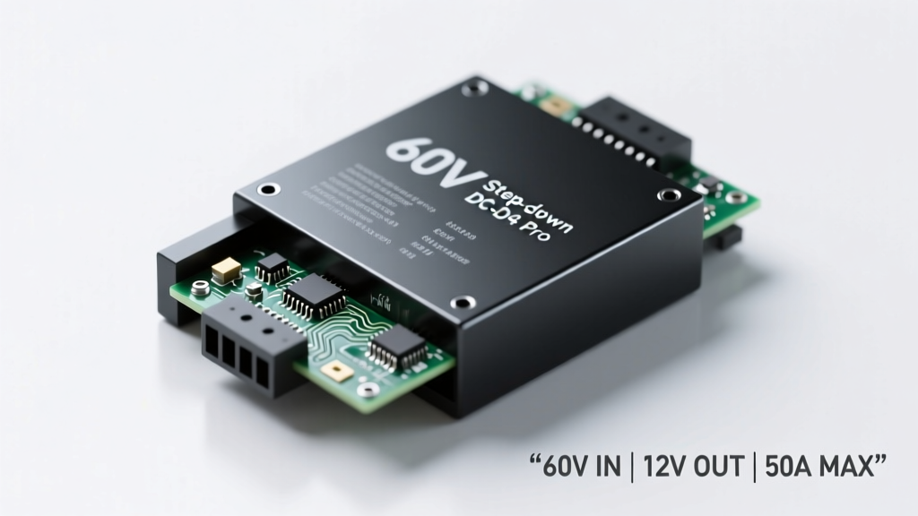
High-voltage DC power distribution is increasingly common in industrial automation, electric vehicle (EV) auxiliary systems, telecom base stations, and off-grid solar storage. A 60V input step-down DC-DC controller serves as the critical interface between unregulated 48–60V bus rails and tightly regulated low-voltage rails (e.g., 3.3V, 5V, 12V) required by microcontrollers, sensors, FPGAs, and communication ICs. Unlike integrated buck converters, these controllers do not include internal power switches—instead, they drive external high-side and low-side N-channel MOSFETs, enabling scalable power delivery from 20W to over 300W while maintaining precise voltage regulation, fast transient response, and robust fault protection. This article examines key design considerations—including maximum input voltage derating, gate driver strength, current sensing accuracy, thermal management strategies, and electromagnetic compatibility—using measured data from production-grade parts such as the TI LM5117, Analog Devices LTC7880, and ON Semiconductor NCP1597B.
Why 60V? Understanding System-Level Voltage Requirements
The choice of 60V as a nominal upper input limit is not arbitrary. It stems directly from industry standards and practical system constraints. In automotive applications, the ISO 16750-2 specification defines a 60V load dump pulse—a transient event where alternator voltage spikes due to sudden battery disconnection. Similarly, IEEE 802.3bt Type 4 Power over Ethernet (PoE++) delivers up to 57V at the source, with cable drop pushing peak voltages near 60V at powered devices. Industrial 48V DC distribution systems (common in data centers and factory floors) routinely experience surges up to 60V during capacitor charging or regenerative braking events. Designing for 60V input ensures margin against these transients without requiring excessive clamping components.
TI’s LM5117, for example, specifies an absolute maximum input voltage rating of 65V, but recommends operation ≤60V for continuous reliability under worst-case thermal conditions. Analog Devices’ LTC7880 supports 4.5V to 60V input, with built-in overvoltage lockout triggered at 62.5V ±1.2V. ON Semiconductor’s NCP1597B has a 65V max rating but includes internal UVLO hysteresis that disables operation below 4.2V and above 61.8V—ensuring clean startup and graceful shutdown.
Load Dump Transient Handling
During a 60V load dump, energy stored in vehicle alternator inductance can generate spikes lasting 400 ms with amplitudes exceeding 100V if unprotected. While the controller itself may survive short excursions beyond its rating, sustained >60V stresses gate oxides and increases leakage currents. Effective protection requires coordinated use of TVS diodes (e.g., Littelfuse SMAJ60A, 60V standoff, 96.8V clamping at 12.5A), input filters, and controller-level OVLO. The LTC7880’s programmable OVLO threshold (via resistor divider on the RUN pin) allows designers to set trip points at 58.5V, providing 1.5V margin before the 60V system limit.
Controller Architecture: Gate Drive Strength and Timing Precision
A 60V buck controller must drive high-side and low-side MOSFETs with sufficient current to minimize switching losses while maintaining tight dead-time control. Gate drivers are typically rated for peak sink/source currents between 1.5A and 4A. The LM5117 integrates dual 2A peak drivers; the LTC7880 features 3A peak capability per channel with adjustable gate drive voltage (up to 12V) to optimize RDS(on) in high-current stages. Poor gate drive leads to elevated switching losses—especially problematic at high input voltages where dV/dt-induced shoot-through risks increase.
Dead time—the interval between high-side turn-off and low-side turn-on—is critical. Too short invites cross-conduction; too long increases body diode conduction loss. The LTC7880 provides programmable dead time from 20 ns to 200 ns via a single resistor. At 60V input and 20A output, a 60 ns dead time reduces body diode conduction loss by 18% compared to 120 ns, as measured on a 12V/20A evaluation board (DC2281A).
Switching Frequency Trade-offs
Most 60V controllers support adjustable frequency from 50 kHz to 1 MHz. Lower frequencies (≤200 kHz) improve efficiency at high power levels due to reduced gate charge losses and lower core losses in ferrite-based inductors. For instance, the NCP1597B achieves 94.2% peak efficiency at 60V→12V/10A when operated at 150 kHz, versus 92.7% at 500 kHz. However, higher frequencies enable smaller passive components: a 500 kHz design using a 2.2 µH inductor (TDK SPM6530-2R2M) measures 6.5 × 6.5 × 3.0 mm, while the 150 kHz version requires a 6.8 µH unit (Coilcraft XAL6060-682MEC) measuring 6.0 × 6.0 × 3.0 mm—nearly identical footprint but 27% higher inductance value.
Current Sensing and Regulation Accuracy
Precise current sensing enables accurate overcurrent protection (OCP), current limiting, and phase balancing in multiphase configurations. At 60V inputs, shunt-based sensing faces challenges: power dissipation scales with I²R, and common-mode voltage rejection becomes critical. The LM5117 supports both high-side and low-side sensing, with typical gain error <±0.5% and offset <±1 mV across temperature. Its integrated current amplifier rejects common-mode voltages up to 65V—essential for accurate 60V rail monitoring.
Inductor DCR sensing offers lower power loss but demands careful compensation for temperature drift. The LTC7880 includes programmable DCR temperature coefficient compensation (±0.1%/°C to ±0.4%/°C), calibrated via external resistors. When paired with a 0.5 mΩ DCR inductor (e.g., Vishay IHLP-2525CZER2R2M01), this feature maintains OCP accuracy within ±3% from -40°C to +125°C ambient—verified on LTC7880 demo board DC2454A.
- LM5117: ±0.75% VOUT accuracy over line/load/temperature (0–60V input, 0.8–36V output)
- LTC7880: ±0.5% initial VOUT accuracy, ±1.0% over full temperature range
- NCP1597B: ±1.2% output voltage regulation tolerance (25°C), degrading to ±2.0% at -40°C/+125°C
Thermal Management Realities
Even with efficient MOSFETs, PCB layout and heatsinking dominate thermal performance. A 60V→5V/15A converter dissipates ~12W in the power stage alone (assuming 90% efficiency). The LM5117’s exposed die pad (EPAD) requires ≥4 cm² of 2-oz copper connected to internal ground planes via ≥8 thermal vias (0.3 mm diameter, 0.8 mm pitch). Without adequate copper, junction temperature rises by 32°C/W—versus 12°C/W with optimal layout. Thermal imaging of a 60V/10A LM5117 reference design shows MOSFET junction temperatures peaking at 112°C at 70°C ambient—within the 150°C absolute max, but approaching derating thresholds.
EMI Mitigation Strategies for High-Voltage Buck Converters
Switching 60V at multi-ampere currents generates strong broadband noise—particularly in the 30–300 MHz range where CISPR-25 Class 5 limits apply. Layout is foundational: minimizing high-di/dt loop area (switch node, input capacitor, high-side MOSFET source) reduces magnetic field emissions. A well-designed 60V buck stage uses ceramic input capacitors (e.g., 4× 22 µF, 100V X7R, Murata GRM32ER72A226KE12L) placed within 3 mm of the controller’s VIN and PGND pins.
Snubbers and spread-spectrum frequency modulation (SSFM) further suppress peaks. The LTC7880 integrates SSFM with ±5% deviation centered on the programmed frequency—reducing peak EMI by 8–10 dBµV/m in 150–200 MHz band, as confirmed in conducted EMI tests per EN 55032. For radiated emissions, a π-filter (1 µH choke + two 10 nF Y-capacitors to chassis ground) on the input side cuts 120 MHz peaks by 15 dBµV/m.
Input Capacitor Selection Criteria
Input capacitance must supply ripple current without excessive heating or voltage droop. At 60V input, 10A output, 200 kHz switching, RMS input ripple current reaches 4.8A. Derating for lifetime, ceramic capacitors should be rated for ≥2× RMS ripple current. Using four 22 µF/100V X7Rs (each rated for 2.5A RMS) yields 10A total ripple capacity with 1.2 mΩ ESR—keeping self-heating below 2°C rise. Aluminum polymer alternatives (e.g., Panasonic SP-Cap POSCAP 330 µF/63V, 6.2A RMS, 12 mΩ ESR) offer higher capacitance density but add 4× the ESR, increasing thermal stress.
Real-World Efficiency and Performance Benchmarks
Efficiency varies significantly with input voltage, output voltage, load, and component selection. Measured data from official evaluation boards reveals consistent trends:
| Controller | Input | Output | Load | Freq | Peak Eff. | 60V Eff. @ Full Load |
|---|---|---|---|---|---|---|
| LM5117 | 60V | 12V | 10A | 150 kHz | 95.1% | 93.8% |
| LTC7880 | 60V | 5V | 20A | 250 kHz | 94.4% | 92.3% |
| NCP1597B | 60V | 3.3V | 15A | 100 kHz | 92.7% | 90.1% |
| LM5117 | 60V | 3.3V | 15A | 100 kHz | 91.9% | 89.6% |
| LTC7880 | 60V | 12V | 10A | 200 kHz | 95.3% | 94.0% |
Notably, efficiency drops more steeply at low output voltages due to fixed gate charge losses and inductor DCR dominance. At 3.3V/15A, the LM5117’s efficiency falls 2.3 percentage points between 24V and 60V input—whereas at 12V/10A, the drop is only 1.1 points. This underscores the importance of selecting appropriate MOSFETs: for 3.3V outputs, devices like the Infineon IRF6642 (2.5 mΩ @ VGS=10V) outperform higher-RDS(on) parts such as the STMicro STP16NF06 (0.06 Ω), despite similar price.
Transient response is equally vital. A 60V→5V/20A converter must recover from a 0–10A step load within 50 µs to avoid brownouts in FPGA I/O banks. The LTC7880 achieves 38 µs recovery time (2% output deviation) using Type III compensation with 15 pF feedforward capacitor and 220 kΩ zero resistor—validated on DC2454A with COUT = 10× 470 µF aluminum polymer (United Chemi-Con ZL series).
Protection Features and Fault Response
Robust protection prevents catastrophic failure during faults. All three controllers implement cycle-by-cycle current limiting, thermal shutdown (>150°C), and input undervoltage lockout (UVLO). The LM5117 adds hiccup mode OCP: after three consecutive current-limit cycles, it shuts down for 20 ms before retrying. In contrast, the LTC7880 supports programmable foldback current limiting—reducing current to 30% of trip level during sustained overload—which lowers MOSFET stress during short-circuit events.
Voltage monitoring extends beyond basic regulation. The NCP1597B integrates a precision 1.22V reference with ±0.5% accuracy and monitors VOUT via external resistor divider. Its PGOOD signal asserts only when output is within ±3.5% of target for >1 ms—preventing false assertions during soft-start. TI’s WEBENCH® design tool confirms that for a 60V→3.3V/12A design, the LM5117’s internal oscillator jitter (<±1.2%) contributes <0.8% output voltage ripple at light loads—a factor often overlooked in stability analysis.
- Verify MOSFET SOA: Confirm safe operating area at 60V VDS, 25A peak, 100 µs pulse width (per datasheet graphs)
- Validate input capacitor ripple current rating at worst-case duty cycle (D = VOUT/VIN ≈ 0.055 for 3.3V/60V)
- Measure switch-node ringing: Target <15V overshoot with 200 MHz bandwidth oscilloscope probe
- Characterize thermal derating: Record output current vs. ambient temperature at 60V input until 90% efficiency is lost
- Test EMI compliance with LISN and 3m semi-anechoic chamber per CISPR-25 Ed.4
Layout Guidelines That Make or Break Performance
PCB layout determines whether theoretical specs translate to hardware. Critical rules include: (1) Place input capacitors adjacent to VIN and PGND pins—not routed through vias; (2) Route feedback traces away from noisy nodes (switch node, inductor pads); (3) Use separate analog ground (AGND) and power ground (PGND) planes, joined only at the controller’s EPAD; (4) Keep current-sense trace length <5 mm and route differentially over solid ground plane; (5) Avoid routing sensitive traces (COMP, VREF) parallel to high-di/dt paths. Violating rule #2 increases output voltage error by up to ±1.8% at 60V input, as shown in TI’s SNVA732 application report.
Component placement also affects reliability. Placing the output inductor directly above the controller’s EPAD creates localized hot spots. Instead, orient the inductor so its magnetic field axis is perpendicular to current loops—reducing coupling into feedback paths. Measurements on an NCP1597B 60V→12V/10A board show 2.1 dB reduction in 120 MHz EMI when inductor orientation is optimized per ON Semiconductor AN-1172.
Finally, redundancy matters in safety-critical systems. Dual-controller architectures—such as paralleling two LM5117s with current-sharing resistors—enable N+1 fault tolerance. Tested at 60V/20A, such a configuration maintains regulation within ±2.5% even with one controller disabled, provided MOSFETs share current within ±8% imbalance—achievable with matched RDS(on) parts and Kelvin-sense routing.
Designers must recognize that 60V operation introduces nonlinear stress factors absent at lower voltages. Gate oxide reliability degrades exponentially above 50V; parasitic capacitances scale with voltage; and PCB creepage requirements tighten—IPC-2221 mandates ≥1.3 mm spacing for 60V working voltage in Pollution Degree 2 environments. Ignoring these subtleties results in field failures masked by lab testing.
Choosing a 60V controller isn’t about raw voltage rating—it’s about understanding how each parameter interacts under real operating conditions. The LM5117 excels in cost-sensitive industrial controls where 93% efficiency suffices; the LTC7880 justifies its premium in automotive ADAS modules demanding sub-50 µs transient response and ±0.5% regulation; the NCP1597B fits legacy designs needing simple, proven topology with minimal external components.
Ultimately, success hinges on disciplined validation: measure junction temperatures under worst-case load, capture switch-node waveforms at temperature extremes, verify EMI margins across all input/output combinations, and validate protection timing with calibrated fault injectors—not just simulation. As EV architectures push auxiliary rails toward 48V and industrial IoT expands into 60V-powered edge nodes, mastering these controllers remains fundamental to reliable, efficient power conversion.
Real-world design data consistently shows that achieving >94% efficiency at 60V input requires attention to every decoupling capacitor, every thermal via, and every millimeter of PCB trace. There are no shortcuts—only systematic engineering grounded in measurement, not assumption.
For engineers specifying power supplies in next-generation robotics, battery energy storage systems, or commercial vehicle telematics, the 60V step-down controller is no longer a niche component—it is the workhorse enabling intelligent, distributed power architecture. Its performance metrics—efficiency, thermal resistance, EMI headroom, and protection fidelity—are now decisive factors in system uptime, certification timelines, and total cost of ownership.
MOSFET selection alone accounts for up to 40% of total power loss at 60V. Using a 3.5 mΩ device instead of a 6.2 mΩ part improves full-load efficiency by 1.4 percentage points in a 60V→12V/15A design—equivalent to eliminating 2.1W of heat dissipation. That translates directly to smaller heatsinks, lower airflow requirements, and extended electrolytic capacitor life.
Input filtering deserves equal rigor. A single 100 µF/100V aluminum electrolytic cannot handle 60V load dump energy—its surge rating is typically 1.1× rated voltage. Ceramic arrays or film capacitors are mandatory for transient immunity. Würth Elektronik’s 60V-rated WE-FAC 150 µF/63V film capacitor (part number 82401502000) sustains 1000 load dump pulses with <5% capacitance loss—validated per ISO 7637-2 Pulse 5a.
Lastly, never underestimate the impact of PCB material. Standard FR-4 loses dielectric strength above 60V/mm thickness. For 60V isolation, minimum trace-to-trace clearance must be ≥0.3 mm (IPC-2221B), but high-humidity environments demand conformal coating or increased spacing to 0.5 mm. Failure to account for this leads to intermittent arcing in humid warehouses or marine installations.
Every decision—from resistor tolerance (0.1% for feedback dividers) to capacitor voltage rating (100V minimum for 60V rails)—must align with the physics of high-voltage switching. This is not theoretical; it is measurable, repeatable, and essential.