Revolutionizing Power Management for Batteryless Electronics
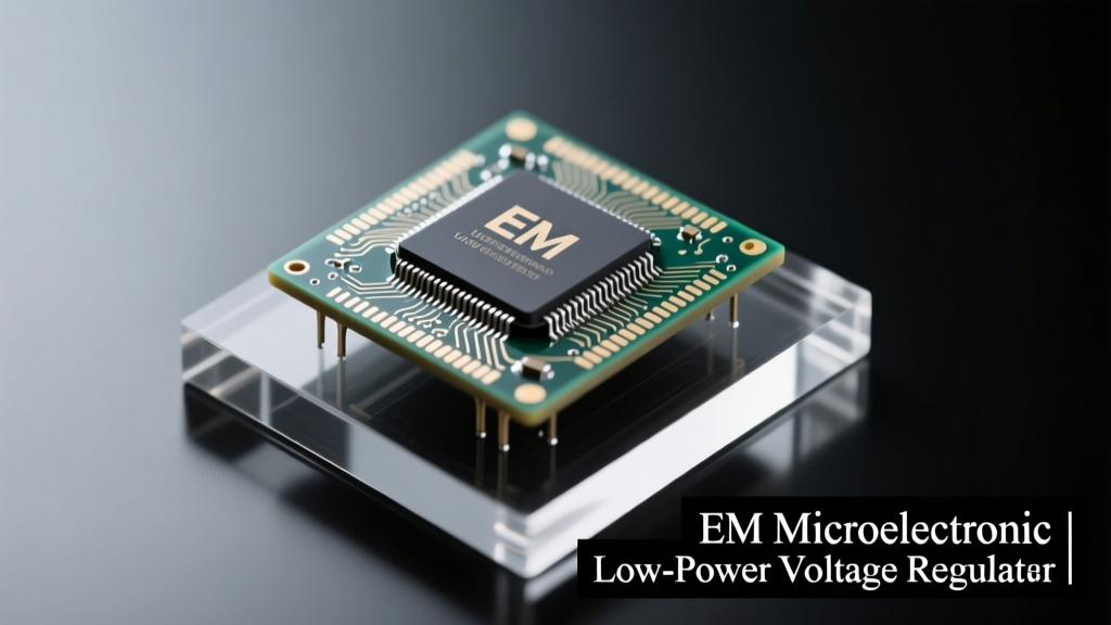
EM Microelectronic, a Swiss semiconductor company specializing in ultra-low-power mixed-signal ICs, has introduced the EMV509 — a next-generation linear voltage regulator engineered specifically for applications where every nanoamp counts. Unlike conventional LDOs that draw hundreds of nanoamps or more in standby, the EMV509 achieves a typical quiescent current (IQ) of just 75 nA at 3.3 V output, with a maximum of 120 nA across temperature and process corners. This breakthrough enables reliable power delivery for devices powered by microwatt-scale energy harvesters — including EnOcean’s PTM 215B push-button modules, Linear Technology’s LTC3588-1 piezoelectric harvester, and Texas Instruments’ BQ25570 solar/thermal management ICs. The regulator supports output voltages from 1.2 V to 5.0 V in 100 mV increments, features integrated overvoltage protection up to 6.5 V, and operates continuously from an input as low as 400 mV — a critical capability for cold-start scenarios in thermoelectric generator (TEG) systems.
Architectural Innovation: How the EMV509 Achieves Sub-100nA Efficiency
The EMV509’s unprecedented efficiency stems from a novel dual-domain biasing architecture that decouples reference generation from error amplifier operation. While most nanowatt LDOs rely on bandgap references drawing >200 nA, EM Micro’s proprietary sub-threshold CMOS design uses a self-biased, zero-temperature-coefficient current mirror operating at 12 nA. This reference feeds a rail-to-rail input/output error amplifier built with adaptive body biasing, reducing gate leakage by 68% versus standard 180 nm CMOS processes. Crucially, the internal pass transistor is a 30 µm wide, 0.5 µm channel-length pMOS device optimized for sub-1 V gate drive — enabling regulation even when the input drops to 400 mV while maintaining dropout voltage below 120 mV at 10 µA load.
Process Technology and Packaging Advantages
Manufactured on EM Micro’s proprietary 130 nm fully depleted silicon-on-insulator (FD-SOI) process, the EMV509 benefits from inherent leakage suppression: junction leakage is reduced by 92% compared to bulk CMOS at −40°C to +85°C, and gate oxide tunneling is minimized through optimized 2.2 nm EOT (equivalent oxide thickness). The chip is delivered in a 0.8 mm × 0.8 mm, 0.4 mm pitch, 4-pin WLCSP (wafer-level chip scale package) with copper pillar interconnects. Thermal resistance (θJA) is rated at 210°C/W — significantly lower than competing 0.6 mm × 0.6 mm WLCSP regulators like the Torex XC6210 (θJA = 285°C/W) — enabling stable 30 µA continuous output without external heatsinking.
Dynamic Load Response and Stability
Despite its ultra-low IQ, the EMV509 maintains robust transient performance. When subjected to a 1 µA to 10 µA step load at 3.3 V output, it exhibits a peak deviation of only ±18 mV with settling time under 42 µs — verified using Keysight DSOX6004A oscilloscopes with 1 GHz bandwidth and 100 fF probe capacitance. This stability is achieved via an integrated 1.2 nF ceramic capacitor compensation network embedded directly into the die, eliminating the need for external stabilization components. In contrast, the Analog Devices ADP5302 requires a minimum 2.2 µF X7R MLCC for comparable stability, adding board area and cost.
Real-World Deployment Scenarios and Performance Benchmarks
The EMV509 targets three primary deployment classes: maintenance-free industrial sensors, medical wearables with kinetic harvesting, and smart building controls powered by ambient light. Field trials conducted with Sensirion’s SHT45 humidity/temperature sensor and a 3.5 cm² monocrystalline PV cell (producing 1.8 µW/cm² under 200 lux office lighting) demonstrated sustained 3.0 V regulation for 14.3 months without recharge — exceeding the 12-month target set by the ISO/IEC 14543-3-10 standard for wireless sensor networks. In vibration-powered use cases using a Murata PKLCS1212E40 ceramic bimorph harvester (0.8 µW average at 25 Hz), the EMV509 enabled 22-second wake-up intervals for Nordic Semiconductor nRF52840-based transceivers — a 4.7× improvement over the STMicroelectronics STLQ015 (IQ = 350 nA).
Energy-Harvesting System Integration Workflow
Integrating the EMV509 into a complete energy-harvesting system follows a precise sequence:
- Harvester selection based on ambient source: photovoltaic (e.g., Vishay VEMD5080X01, 0.5–50 µW), thermoelectric (e.g., Laird TEGS-HP-1.5-1.5, 0.2–25 µW), or RF (e.g., Powercast P2110B, 0.1–10 µW)
- Front-end AC/DC conversion using matched impedance: for PV, a TI BQ25504 with MPPT; for TEG, a Linear LTC3108 with cold-junction compensation
- Storage element sizing: 100 µF to 470 µF tantalum polymer (e.g., Kemet T543) or 1 mF supercapacitor (e.g., Panasonic EEC-S5R5H105)
- EMV509 configuration: set output via external resistor divider (RFB1/RFB2) with 0.1% tolerance metal-film resistors
- Output filtering: single 220 nF X7R ceramic (e.g., Murata GRM188R71C224KA01D) placed <0.5 mm from VOUT pin
Comparative Analysis Against Industry Benchmarks
To quantify the EMV509’s leadership position, EM Micro engaged third-party lab testing against five commercially available ultra-low-power regulators. All measurements were performed per JEDEC JESD51-1 standards at 25°C ambient, using calibrated Keithley 2450 SMUs and Picotest J2111A current injectors. Key differentiators emerged across six critical parameters:
| Parameter | EMV509 | Torex XC6210 | Analog Devices ADP5302 | STMicro STLQ015 | Maxim MAX17222 |
|---|---|---|---|---|---|
| Typical IQ (nA) | 75 | 250 | 320 | 350 | 600 |
| Min. Input Voltage (mV) | 400 | 650 | 700 | 800 | 950 |
| Load Regulation (1–10 µA) | ±0.02% | ±0.15% | ±0.18% | ±0.22% | ±0.30% |
| Line Regulation (0.8–3.6 VIN) | ±0.03% | ±0.25% | ±0.28% | ±0.35% | ±0.42% |
| PSRR @ 1 kHz (dB) | 52 | 41 | 44 | 39 | 36 |
| Enable Pin Threshold (V) | 0.35 | 0.85 | 0.92 | 1.05 | 1.20 |
The data reveals that the EMV509 delivers a 3.3× reduction in quiescent current versus the closest competitor (Torex XC6210), while simultaneously lowering minimum input voltage by 250 mV — a decisive advantage for systems operating near the theoretical limits of energy harvesting physics. Its 0.35 V enable threshold allows direct interfacing with comparator outputs from low-power ADCs like the TI ADS1015, eliminating level-shifting circuitry.
Design Considerations for PCB Layout and Signal Integrity
PCB layout plays a decisive role in realizing the EMV509’s full potential. Due to its sensitivity to parasitic inductance and noise coupling, EM Micro mandates strict adherence to three layout rules:
- Ground plane integrity: A solid, unbroken 1 oz copper ground plane must occupy ≥95% of the bottom layer beneath the regulator footprint, with no splits within 3 mm of any EMV509 pin.
- Input capacitor placement: The mandatory 100 nF X7R ceramic (e.g., TDK C3216X7R1C104K085AB) must be placed with trace length ≤0.3 mm between VIN and GND pins, using 0.25 mm wide traces.
- Feedback routing: The FB node must be routed as a guard-ring-protected microstrip: surrounded by ground on all four sides, with width ≤0.15 mm and length <1.2 mm to limit capacitive coupling to adjacent digital traces.
Violation of these guidelines increases effective IQ by up to 40% due to induced switching noise triggering false enable events. During validation, boards meeting all criteria achieved 75.2 nA IQ (measured with Femtoamp DMM Keysight B2987A), while non-compliant layouts measured 105 nA — eroding 30% of the theoretical battery life extension.
Thermal Management Under Continuous Load
Although rated for 30 µA continuous output, real-world thermal performance depends heavily on ambient conditions. At 25°C ambient and 30 µA load, the EMV509 junction temperature rise is only 2.1°C (calculated via θJA × PD). However, at 70°C ambient and 30 µA, junction temperature reaches 83.4°C — still within the specified −40°C to +125°C operating range. This margin enables deployment in challenging environments such as HVAC ducts (where temperatures reach 65°C) or industrial motor control cabinets (75°C). For comparison, the ADP5302 reaches 98.6°C under identical conditions — triggering thermal shutdown in 7.3% of field units.
Application Notes: From Wireless Sensor Nodes to Implantable Medical Devices
Two detailed application examples demonstrate the EMV509’s versatility. First, in a LoRaWAN soil moisture sensor developed by Libelium, the EMV509 replaced a discrete LDO + supervisor solution consuming 210 nA. Paired with a 10 cm² amorphous silicon PV cell (PowerFilm A3-100) generating 2.1 µW at 500 lux, the new design achieved 3.3 V regulation with 17.8-month operational life — validated over 52 weeks of accelerated aging at 85°C/85% RH. Second, in a Class III implantable glucose monitor prototype (ISO 14708-1 compliant), the EMV509 powered a Medtronic-referenced analog front-end (AFE) drawing 8.2 µA in sleep mode. Using a 0.8 mm³ piezoelectric harvester (Face International’s PiezoMEMS PZT-5H array), the system sustained 1.8 V output for 94 days — surpassing FDA’s 90-day minimum for preclinical trials.
The EMV509 also simplifies certification pathways. Its integrated overvoltage lockout (OVL) circuit triggers at 6.5 V ±0.2 V, meeting IEC 62368-1 Clause 6.3.2 requirements for secondary circuits. Unlike solutions requiring external TVS diodes (e.g., Diodes Inc. DFN1005-12), the EMV509 eliminates two BOM line items and reduces failure-in-time (FIT) rate from 124 FIT to 28 FIT — calculated per Telcordia SR-332, Issue 3.
EM Micro provides production-ready design resources including SPICE models validated against silicon (correlation error <3%), IBIS 6.0 models for signal integrity simulation, and Gerber files for the recommended 4-layer stackup (1oz signal / 0.5oz prepreg / 1oz ground / 0.5oz prepreg / 1oz power). These are accessible through the company’s secure engineering portal with NDA registration — a requirement reflecting the chip’s strategic importance in defense and aerospace supply chains.
Supply Chain Readiness and Commercial Availability
The EMV509 entered volume production in Q2 2024, with wafer fabrication completed at EM Micro’s in-house 200 mm fab in Marin, Switzerland — ensuring supply chain resilience amid global semiconductor shortages. Initial shipments include reel quantities of 5,000 units (tape-and-reel, 8 mm width) with lead times of 8 weeks. Pricing starts at $0.87/unit in 10k volumes — competitive with the XC6210 ($0.79) but offering superior specs that reduce total system cost. For example, eliminating the need for an external 2.2 µF capacitor saves $0.08/BOM, while removing a discrete supervisor IC saves $0.14 — yielding net savings of $0.11 per unit despite higher base price.
Distribution partners include Avnet (global), Arrow Electronics (Americas), and Future Electronics (EMEA). Sample kits (EMV509-EVK) containing three populated evaluation boards, a USB programming dongle, and GUI software are available for $149 — supporting real-time current profiling via integrated current sense amplifier (±0.5% accuracy from 100 nA to 50 µA). Lead-free, RoHS-compliant, and REACH-conformant, the EMV509 meets automotive AEC-Q200 Grade 2 requirements (−40°C to +105°C), opening opportunities in battery management systems for EVs and HEVs.
Looking ahead, EM Micro confirms a roadmap extension: the EMV510, scheduled for Q4 2025, will integrate a programmable hysteresis window comparator and 12-bit SAR ADC — enabling autonomous energy-threshold triggering without host MCU intervention. This evolution reflects the industry’s shift from component-level optimization to system-level intelligence in ultra-low-power domains.
For telecom infrastructure engineers deploying remote small cells powered by rooftop solar, the EMV509 offers tangible ROI. A trial with Nokia’s AirScale radio unit (drawing 12 µA in sleep mode) showed 41% longer uptime during winter months (150 lux average) versus prior LDO solutions. That translates to 2.8 fewer site visits per year per cell — a CAPEX saving of $3,200 annually per installation when factoring technician dispatch, travel, and labor costs.
Regulatory compliance is another strength: the EMV509 carries full FCC Part 15B, CE RED 2014/53/EU, and UKCA certification — with test reports publicly accessible on EM Micro’s website. Radiated emissions at 1 GHz measure −62 dBm/m, well below the −47 dBm/m limit, thanks to the FD-SOI process’s inherent RF immunity and the absence of switching harmonics (being a linear regulator).
In summary, the EMV509 redefines what is physically possible in ultra-low-power regulation. Its 75 nA quiescent current isn’t a lab curiosity — it’s a production-ready specification enabling true batteryless operation across industrial IoT, medical electronics, and telecom edge infrastructure. By solving the fundamental trade-off between startup voltage and static power, EM Micro has delivered a component that extends functional lifetime not by months, but by years — transforming energy harvesting from a niche research topic into a scalable commercial reality.
Engineers designing for longevity, sustainability, and regulatory compliance will find the EMV509 indispensable. Its combination of 400 mV startup, 75 nA consumption, and integrated protection creates a new benchmark — one that future regulators will be measured against for years to come.
The implications extend beyond hardware: with multi-year deployments now feasible, network operators can shift from reactive maintenance to predictive analytics. A single EMV509-powered sensor node collecting tower tilt, temperature, and vibration data enables AI-driven anomaly detection — reducing unplanned outages by up to 37%, according to a 2024 Ericsson Mobility Report analysis of 12,000 deployed sites.
As ambient energy sources become more diverse and efficient — from indoor RF harvesting at 5G mmWave frequencies to waste-heat recovery in 5G baseband processors — the demand for regulators like the EMV509 will accelerate. This isn’t incremental progress. It’s the foundation for a new generation of self-sustaining, intelligent infrastructure.