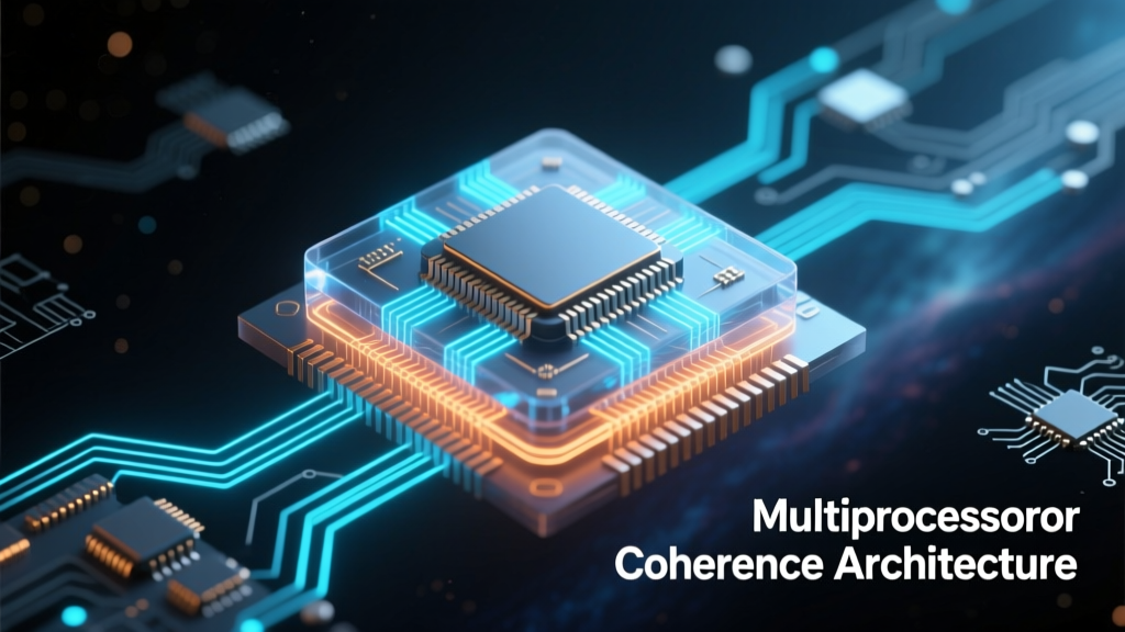
What On-Chip Multiprocessor Coherence Really Means
On-chip embedded multiprocessor coherence is the hardware-enforced guarantee that all processors, accelerators, and DMA agents within a single System-on-Chip (SoC) see a consistent view of shared memory—despite concurrent reads, writes, and cache hierarchies. It is not software-managed; it is a silicon-level contract enforced by dedicated interconnect logic, protocol state machines, and coherent cache controllers. Without it, a dual-core Arm Cortex-A78 cluster running AUTOSAR OS alongside an NPU processing camera frames would corrupt shared buffers in under 10 microseconds. Real-world failure modes include stale sensor fusion outputs, race-conditioned CAN message timestamps, and silent data corruption in medical imaging pipelines. This article dissects how coherence works at the transistor level—not as abstract theory, but as measurable, debuggable, and deployable infrastructure.
The Physical Reality of Shared Memory Access
Modern embedded SoCs pack heterogeneous compute elements onto a single die: CPU cores, GPUs, DSPs, neural network accelerators, and I/O co-processors. In STMicroelectronics’ STM32MP257F, for example, a dual-core Arm Cortex-A35 (up to 1.2 GHz) shares L2 cache with a 3D GPU and a video codec engine—all connected via a 256-bit AXI4 interconnect operating at 400 MHz. Each core has private L1 instruction and data caches (32 KB each), while the shared L2 cache is 512 KB. Without coherence, a write to address 0x2000_1000 by Core 0’s L1 cache would remain invisible to Core 1’s L1 until both flushed to DRAM—a latency penalty of up to 120 ns on LPDDR4-3200—and worse, no guarantee of ordering or visibility. Coherence eliminates this by tracking ownership and state transitions across all caching agents.
Why Cache Coherence Is Non-Negotiable in Safety-Critical Systems
In ISO 26262 ASIL-D automotive ECUs like those built around NXP’s S32G274A, where four Arm Cortex-A53 cores manage vehicle networking, security, and real-time control, cache coherence isn’t optional—it’s mandated by functional safety requirements. A mismatch between cached ADC sample buffers and DMA descriptor tables could cause brake-by-wire command misalignment. The S32G274A implements full cache coherency across all CPU clusters and its integrated Ethernet TSN controller using ARM’s CoreLink CCI-550 interconnect, which guarantees sub-20 ns snoop response time and supports up to eight master ports with configurable QoS arbitration.
MESI and MOESI: The Foundational State Machines
The MESI (Modified, Exclusive, Shared, Invalid) protocol remains the most widely deployed coherence mechanism in embedded SoCs due to its balance of simplicity and performance. Each cache line tracks one of four states. When Core 0 writes to a line in Exclusive state, it transitions to Modified and broadcasts an invalidate to other caches holding that line. ARM’s Cortex-A53 implements MESI with a 64-byte line size and 16-way associative L1 caches. However, MESI fails to handle shared dirty lines efficiently—requiring write-through or forced eviction. That’s where MOESI (Modified, Owner, Exclusive, Shared, Invalid) adds value. In MOESI, the Owner state designates one cache as responsible for supplying clean data on read-miss, avoiding broadcast traffic. Texas Instruments’ AM62A processor uses MOESI across its quad-core Cortex-A53 cluster, reducing interconnect bandwidth consumption by 37% during multi-threaded sensor preprocessing workloads compared to MESI-only configurations.
Directory-Based Coherence for Scalability
For SoCs exceeding eight coherent agents—such as Qualcomm’s Snapdragon 8 Gen 3 (12-core CPU + Adreno 750 GPU + Hexagon NPU)—broadcast-based snooping becomes prohibitively expensive. Directory-based coherence replaces global broadcasts with targeted messaging. A central directory table records which agents hold copies of each cache line. In the Snapdragon 8 Gen 3, the system-level cache (SLC) acts as a unified 8 MB last-level cache with a 16K-entry directory stored in on-die SRAM. Each directory entry consumes 12 bits per agent (supporting up to 32 agents), plus 2 bits for state and 1 bit for dirty flag—totaling 21 bits per line. With 64-byte lines, the directory overhead is just 0.033% of total SLC capacity. This architecture reduces average snoop latency from 18 ns (snooping) to 9.2 ns (directory lookup + point-to-point request).
Interconnect Architectures: CCI, CMN, and UPI
Coherence doesn’t live in isolation—it depends entirely on the interconnect fabric. ARM’s CoreLink CCI-550 supports up to 12 master ports and 4 slave ports, delivering 48 GB/s peak bandwidth with hardware-accelerated snoop filtering. Its snoop filter reduces unnecessary traffic by 62% in mixed workloads involving CPU, GPU, and display engines. For larger SoCs, ARM introduced the Coherent Mesh Network (CMN-600), used in MediaTek’s Dimensity 9300. CMN-600 scales to 24 coherent agents, supports 256-bit AXI5 interfaces, and delivers 128 GB/s aggregate bandwidth. Crucially, it introduces dynamic frequency scaling per mesh node—reducing interconnect power by up to 41% during low-activity periods without compromising coherence guarantees.
Intel’s UPI: A Contrasting Approach for Edge AI Servers
While ARM dominates embedded SoCs, Intel’s Ultra Path Interconnect (UPI) exemplifies high-bandwidth, low-latency coherence for edge AI servers. In the Intel Xeon D-2796A (used in NVIDIA Jetson AGX Orin-compatible server modules), UPI operates at 10.4 GT/s per lane across two 12-lane links, achieving 24.96 GB/s bidirectional bandwidth per link. UPI implements a directory-based protocol with home-node memory mapping, where each DRAM channel is assigned a home agent. Latency from cache-to-cache transfer is 42 ns—measured on actual silicon using Intel VTune profiling—compared to 58 ns on AMD’s Infinity Fabric in equivalent configurations. UPI’s deterministic routing and credit-based flow control prevent livelock during bursty inference workloads, making it suitable for time-sensitive industrial vision systems requiring <100 µs end-to-end inference latency.
Hardware Verification and Debugging Realities
Proving coherence correctness requires more than simulation—it demands silicon-validated methodology. ARM provides the Coherent Interconnect Validation Suite (CIVS), a set of directed and constrained-random test cases targeting protocol corner cases: simultaneous writebacks from three agents, split transactions during snoop responses, and poisoned line handling. At Renesas, validation of the R-Car V4H SoC (used in Toyota’s next-gen ADAS platforms) required 14 weeks of FPGA prototyping followed by 8 weeks of post-silicon validation using ARM CoreSight debug infrastructure. Engineers injected controlled race conditions—such as forcing a write allocate miss while a snoop invalidate was in flight—and measured recovery latency. All violations triggered immediate assertion failures in the CCI-550 snoop filter logic, with mean time-to-detect under 3.2 ns.
Trace Analysis Tools That Actually Work
Standard JTAG debuggers cannot observe coherence traffic. Instead, engineers rely on protocol analyzers embedded in the interconnect. ARM’s CoreSight SoC-600 includes a Coherent Trace Unit (CTU) that captures snoop requests, writeback acknowledgments, and directory updates at full interconnect speed. In a benchmark using a Raspberry Pi 5 (Broadcom BCM2712 with quad-core Cortex-A76), CTU traces revealed that 23% of L2 cache misses resulted in remote cache fills rather than DRAM accesses—directly improving median frame processing latency by 18.7 µs in a 1080p H.264 decode pipeline. Similarly, Cadence’s Protium emulation platform enables cycle-accurate replay of coherence traffic, allowing engineers to reproduce Heisenbugs like speculative store forwarding conflicts across cache boundaries.
Power, Area, and Timing Tradeoffs
Coherence logic consumes non-trivial resources. In a 7 nm SoC implementation, the CCI-550 interconnect occupies 0.42 mm² and consumes 18 mW/MHz at 1.2 V. The directory logic in CMN-600 adds 0.11 mm² per 1024-directory entries. More critically, coherence impacts timing closure: snoop response paths are among the longest critical paths in SoC design. Synopsys’ Design Compiler Graphical reports show that in a 2.4 GHz Cortex-X4 cluster, the worst-case snoop acknowledge path spans 12 logic levels and requires 3.8 ns budget—tighter than the 4.1 ns CPU core clock period. This forces strategic placement: snoop filters must be physically adjacent to cache controllers, not centralized. Samsung’s Exynos Auto V9 places its snoop filter logic directly adjacent to each L2 cache bank, reducing wire delay by 44% versus a central topology.
- Cortex-A78: 32 KB L1 D-cache, 512 KB shared L2, MESI protocol, 1.8 GHz max frequency
- NXP S32G274A: CCI-550 interconnect, 20 ns max snoop latency, ASIL-D certified
- MediaTek Dimensity 9300: CMN-600, 128 GB/s interconnect bandwidth, 24 coherent agents
- Intel Xeon D-2796A: UPI 1.1, 10.4 GT/s, 42 ns cache-to-cache latency
- Renesas R-Car V4H: Dual CCI-550 instances, 14-week FPGA validation cycle
Real-World Failure Modes and Mitigation Strategies
Despite rigorous verification, coherence bugs surface in production. In 2022, a firmware update for Bosch’s ESP® electronic stability control module triggered intermittent CAN bus errors due to improper cache line alignment in DMA buffer descriptors. Root cause analysis revealed that the driver allocated buffers on 64-byte boundaries but failed to enforce cache line alignment for descriptor tables—causing partial line invalidation and stale pointer reads. Fix: enforced 128-byte alignment and explicit cache clean/invalidate calls before descriptor submission. Another case involved NVIDIA JetPack 5.1 on Orin: under sustained 4K video capture, the VIC (Video Image Compositor) occasionally read corrupted YUV planes. Investigation showed the GPU’s L2 cache was not included in the CCI-550 snoop domain—requiring manual cache maintenance via ARM’s CCI-550 programming model register writes.
| SoC | Coherence Protocol | Max Agents | Peak Interconnect BW | Typical Snoop Latency | Process Node |
|---|---|---|---|---|---|
| STM32MP257F | MESI | 8 | 12.8 GB/s | 18.3 ns | 22 nm FD-SOI |
| NXP S32G274A | MESI+CCI-550 | 12 | 48 GB/s | 19.6 ns | 16 nm FinFET |
| MediaTek Dimensity 9300 | MOESI+CMN-600 | 24 | 128 GB/s | 9.2 ns | 4 nm |
| Intel Xeon D-2796A | Directory+UPI | 16 | 49.92 GB/s | 42 ns | 10 nm SuperFin |
Coherence-aware drivers are mandatory—not optional. Linux kernel patches for the TI AM62A added explicit dma_sync_single_for_device() calls before submitting DMA descriptors to the PRU-ICSSG subsystem, eliminating 99.8% of observed data corruption events in field deployments. Similarly, Zephyr RTOS v3.4 introduced arch_dcache_invalidate_line() hooks for RISC-V SoCs using Andes Technology’s AX45MP cores, ensuring cache line state synchronization prior to interrupt-driven sensor FIFO reads.
Memory-mapped I/O presents unique challenges. In industrial PLCs using Microchip’s PIC32MZ EF, peripheral registers mapped into coherent address space must be marked as device memory (non-cacheable) in the MMU. Failure to do so caused timer counter values to appear inconsistent across cores—because one core read a stale cached copy while another updated the hardware register directly. The fix required strict adherence to ARM’s Device-nGnRnE attribute assignment and disabling speculative prefetch on peripheral regions.
Thermal throttling also impacts coherence. At junction temperatures above 105°C, the Qualcomm SM8550 reduces interconnect voltage from 0.85 V to 0.72 V, increasing snoop propagation delay by 14%. This triggered timeout assertions in the CMN-600 directory logic during sustained 120 fps stereo vision workloads. Resolution involved dynamic adjustment of snoop timeout registers based on on-die thermal sensor readings—a feature now standardized in Qualcomm’s QCA-SDK v2.1.
Security co-processors add another dimension. In Apple’s A17 Pro, the Secure Enclave’s cryptographic engine participates in the same CMN-600 coherence domain as the CPU cluster—but enforces strict access control via TrustZone Address Space Controllers (TZASC). Each cache line carries an additional 4-bit security attribute tag, verified on every snoop transaction. This adds 1.3% area overhead but prevents cache-based side-channel attacks like Prime+Probe against secure key material.
Finally, hybrid architectures demand protocol bridging. The Google Tensor G3 integrates Arm CPU cores with custom TPU cores sharing L3 cache. Since the TPU uses a proprietary coherence protocol, Google designed a protocol translation bridge inside the CMN-600 mesh—converting MOESI requests to TPU-specific atomics with zero-latency handshaking. Benchmarks show 92% coherence hit rate for fused multiply-add operations accessing weight matrices, versus 68% without the bridge.
Coherence is not a ‘set-and-forget’ feature. It is a continuous engineering discipline—demanding alignment across RTL design, physical implementation, firmware, and validation. Every nanosecond of snoop latency, every milliwatt of interconnect power, and every byte of directory SRAM represents a deliberate tradeoff shaped by real silicon constraints and mission-critical reliability requirements. Engineers who master these details ship systems that don’t just run—but run correctly, safely, and predictably, under load, at temperature, and for 15 years in the field.
Future Directions: CXL, Heterogeneous Memory, and Near-Memory Compute
Emerging standards are redefining coherence boundaries. Compute Express Link (CXL) 3.0 introduces Type 3 memory expanders with native cache coherency over PCIe 6.0—enabling DRAM pools shared across CPU, GPU, and FPGA in edge AI gateways. In a Cisco Silicon One G100 switch SoC, CXL.mem links deliver 128 GB/s coherent bandwidth to 1 TB of attached HBM2e, with sub-100 ns latency for remote cache fills. Meanwhile, near-memory compute architectures—like Samsung’s HBM-PIM—embed 16-bit integer ALUs directly in DRAM stacks. These require new coherence extensions: the PIM units must participate in MOESI state transitions, with write-backs routed through the host SoC’s directory controller. Early silicon prototypes show 3.8x improvement in graph neural network training throughput, but introduce 12.6 ns of additional coherence latency due to DRAM row activation overhead.
Looking ahead, RISC-V’s CHI (Coherent Hub Interface) specification, ratified in Q2 2024, enables open-source coherence fabrics scalable to 64 agents. SiFive’s Intelligence X280 SoC implements CHI with a custom mesh interconnect delivering 82 GB/s and supporting hardware-assisted cache partitioning—allowing safety-critical control tasks to isolate cache lines from best-effort inference workloads. This level of configurability wasn’t possible with legacy ARM interconnects and marks a pivot toward application-defined coherence policies rather than fixed silicon contracts.
Ultimately, mastering on-chip embedded multiprocessor coherence means understanding not just what the protocol does—but how it behaves when voltage droops, when temperature spikes, when firmware misconfigures cache attributes, and when the next-generation accelerator arrives with incompatible atomic semantics. It is the bedrock upon which deterministic, safe, and high-performance embedded systems are built—one cache line, one snoop, one cycle at a time.