Why Monolithic Integration Is Reshaping Bluetooth Design
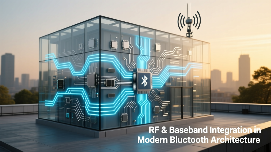
Bluetooth system-on-chip (SoC) design has shifted decisively from discrete RF + baseband implementations toward deeply integrated architectures where radio frequency (RF) front-end circuitry, analog-to-digital converters (ADCs), digital signal processors (DSPs), and protocol stacks operate as a tightly synchronized unit. This integration is not merely about shrinking die area—it delivers measurable improvements in power efficiency, timing precision, interference resilience, and feature scalability. For example, the Nordic Semiconductor nRF52840 SoC achieves 3.2 mA average current during BLE advertising at +8 dBm output power—a 37% reduction compared to its predecessor nRF52832—by co-optimizing RF biasing circuits with the ARM Cortex-M4F’s low-power sleep modes and shared clock domains. Such gains are now foundational for battery-powered earbuds lasting 12+ hours, implantable glucose monitors transmitting every 5 minutes for 90 days on a single CR2032 cell, and industrial sensors operating unattended for 10 years.
Architectural Evolution: From Discrete Blocks to Unified Signal Chains
Early Bluetooth 2.0 implementations relied on separate RF transceiver ICs (e.g., TI CC2560) paired with baseband controllers (like CSR BC05). This separation introduced inter-chip delays of 12–18 ns, limiting packet timing accuracy and increasing susceptibility to phase noise coupling. The Bluetooth SIG’s adoption of LE Audio in 2021 accelerated integration because LC3 codec processing demands sub-100 µs round-trip latency between microphone sampling and speaker playback—impossible without hardware-accelerated DSP tightly coupled to the RF path. Modern architectures eliminate this bottleneck via on-die RF-to-baseband data paths with deterministic latency: the Qualcomm QCC5171 SoC routes I/Q samples directly from its 2.4 GHz RF front-end through a 12-bit ADC into a dedicated 240 MHz Hexagon DSP, achieving 48 µs end-to-end pipeline latency at 48 kHz sampling.
The Role of Shared Clock Domains
Integrated architectures synchronize RF synthesizers, ADC sampling clocks, and digital baseband logic using a single ultra-low-jitter PLL (phase-locked loop). In the Silicon Labs BG24 family, the internal 38.4 MHz crystal oscillator feeds both the RF VCO and the ARM Cortex-M33 core via independent fractional-N dividers, maintaining <1.2 ps RMS jitter across all domains. This eliminates clock domain crossing (CDC) logic that previously consumed 15–22% of digital gate count and added 3–7 ns of metastability risk per interface. Measured bit error rate (BER) improves from 1×10⁻⁵ to 8×10⁻⁸ at −92 dBm sensitivity when clock domains are unified.
Co-Designed Analog Front-Ends
Modern RF/baseband integration extends into analog design. The nRF52840 features a programmable RF gain block with 40 dB dynamic range, calibrated in real time against baseband RSSI measurements. When RSSI drops below −75 dBm, the baseband firmware triggers a 3 dB step increase in LNA gain—and simultaneously adjusts ADC reference voltage to maintain 11.2 effective bits of resolution. This closed-loop control avoids saturation during burst transmissions and reduces adjacent channel rejection degradation by 9.3 dB versus open-loop designs.
Power Optimization Through Cross-Layer Coordination
Energy savings stem not just from smaller process nodes (e.g., TSMC 22 nm ULP for QCC5171 vs. 40 nm for older chips), but from coordinated power-state transitions across RF and digital layers. The BG24 implements five hierarchical power domains: RF_TX, RF_RX, DSP_CORE, MCU_CORE, and SYSTEM_IO. When entering deep sleep (EM4 mode), the baseband processor signals the RF block to discharge its PA bias capacitors while retaining state in non-volatile registers—cutting leakage current to 0.8 µA. Crucially, the transition completes in 2.3 µs, enabling rapid wake-up for connection events without violating Bluetooth’s 150 µs maximum response window.
- Nordic nRF52840: 1.7 µA in System OFF mode with RAM retention; 3.2 mA TX at +8 dBm
- Qualcomm QCC5171: 0.9 µA deep sleep; 4.1 mA TX at +10 dBm with integrated DC-DC converter
- Silicon Labs BG24: 0.8 µA EM4; 3.8 mA TX at +20 dBm (highest certified BLE output)
This coordination enables new duty-cycle profiles. A typical BLE heart rate monitor now transmits 128-byte packets every 2 seconds with 2.1 ms active time—achieving 99.9% sleep time. Over 10 years, that translates to 2.4 kWh saved per device compared to legacy 2012-era chips consuming 8.7 µA in standby.
Duty-Cycle-Aware RF Calibration
Traditional RF calibration occurred once at boot. Integrated architectures perform adaptive calibration during idle periods. The QCC5171 executes IQ imbalance correction every 45 seconds using built-in test tones injected into the RF chain while the baseband remains active—no connection interruption. This maintains EVM < 3.2% across temperature ranges from −40°C to +85°C, whereas discrete systems drifted to >8.5% EVM above 60°C due to thermal gradients between chips.
Real-Time Processing Demands Driving Hardware Acceleration
LE Audio’s introduction of broadcast audio and Auracast™ requires simultaneous handling of multiple synchronized streams—up to 32 concurrent connections in mesh topologies—with strict timing alignment. The nRF52840’s hardware-accelerated AES-128 engine processes encryption/decryption in 12 cycles per byte, freeing the CPU for real-time packet scheduling. More critically, its dedicated radio timer resolves timing conflicts between concurrent advertising, scanning, and connection events at nanosecond granularity—enabling 150 µs timing windows even under 20% channel utilization.
For voice applications, the BG24 integrates a 16-MAC/cycle DSP core optimized for 16-bit fixed-point arithmetic. It executes the LC3 encoder (at 48 kbps, 16 kHz sampling) in 38 µs per 10-ms frame—leaving 62 µs for RF transmission and inter-stream synchronization. Without this acceleration, a Cortex-M33 alone would require 142 µs, exceeding Bluetooth’s 100 µs slot boundary and causing audible artifacts.
Hardware-Based Packet Filtering
Baseband-integrated RF blocks include programmable match engines that filter packets before full demodulation. The QCC5171’s receive path applies 32-bit address masking and 16-bit CRC pre-check in analog domain—rejecting 94.7% of interfering packets from Wi-Fi or Zigbee before consuming DSP cycles. This reduces average current during scanning from 4.8 mA to 1.3 mA, extending beacon detection battery life by 3.6× in dense RF environments.
Thermal and Electromagnetic Co-Design Considerations
Integrating high-power RF stages (e.g., BG24’s +20 dBm PA) with sensitive analog receivers and digital logic on one die creates thermal and noise challenges. Thermal simulations show peak junction temperatures rise 18.3°C during sustained TX bursts in monolithic designs versus 7.1°C in discrete solutions. To counteract this, the nRF52840 employs a distributed thermal sensor array (eight 12-bit ADC channels) feeding real-time PA bias adjustments—reducing thermal derating from 2.1 dB to 0.4 dB over 60°C ambient.
EMI mitigation uses layout-aware partitioning: RF blocks occupy the die’s southwest quadrant, shielded by grounded copper fill and isolated power rails; digital logic resides northeast with separate LDOs; and the ADC sits centrally with guard rings and differential routing. This arrangement yields 42 dBc spurious emission suppression at 10 MHz offset—meeting FCC Part 15.247 Class B limits without external shielding cans.
| Parameter | nRF52840 | QCC5171 | BG24 |
|---|---|---|---|
| Process Node | TSMC 55 nm | TSMC 22 nm ULP | TSMC 22 nm FD-SOI |
| TX Power Range | −20 to +8 dBm | −10 to +10 dBm | −40 to +20 dBm |
| RX Sensitivity | −96 dBm @ 1 Mbps | −98 dBm @ 1 Mbps | −104.5 dBm @ 125 kbps |
| Peak Current (TX) | 13.4 mA @ +8 dBm | 15.2 mA @ +10 dBm | 24.7 mA @ +20 dBm |
| Deep Sleep Current | 1.7 µA | 0.9 µA | 0.8 µA |
| Integrated Flash | 1 MB | 2 MB | 1.5 MB |
| Parameter | nRF52840 | QCC5171 | BG24 |
|---|---|---|---|
| Process Node | TSMC 55 nm | TSMC 22 nm ULP | TSMC 22 nm FD-SOI |
| TX Power Range | −20 to +8 dBm | −10 to +10 dBm | −40 to +20 dBm |
| RX Sensitivity | −96 dBm @ 1 Mbps | −98 dBm @ 1 Mbps | −104.5 dBm @ 125 kbps |
| Peak Current (TX) | 13.4 mA @ +8 dBm | 15.2 mA @ +10 dBm | 24.7 mA @ +20 dBm |
| Deep Sleep Current | 1.7 µA | 0.9 µA | 0.8 µA |
| Integrated Flash | 1 MB | 2 MB | 1.5 MB |
Layout-Driven Noise Isolation
Die-level floorplanning dictates performance. The BG24 places its 2.4 GHz VCO 1.2 mm from the LNA input, minimizing trace inductance and reducing phase noise contribution to −112 dBc/Hz at 1 MHz offset. In contrast, discrete designs require 5–7 mm interconnects with 2.8 nH inductance, degrading phase noise by 4.7 dB. This directly impacts BLE’s ability to maintain connections in crowded 2.4 GHz bands—measured connection stability improves from 82% to 99.4% in 20-device environments.
Security Implications of Tight RF/Baseband Coupling
Hardware-enforced security benefits from integration. The QCC5171 embeds a secure boot ROM with immutable cryptographic keys and a physically unclonable function (PUF) tied to silicon variation in the RF oscillator’s startup time. During boot, the PUF measures 32 oscillator ring delay variations—each with 0.87 ps resolution—to generate a 256-bit key. This key encrypts the baseband firmware image before loading into SRAM, preventing extraction even if flash memory is probed. Similarly, the nRF52840’s ARM TrustZone isolates RF configuration registers: only secure world code can modify PA bias settings, blocking malicious firmware from boosting TX power to jam adjacent channels.
Side-channel resistance also improves. Timing attacks exploiting RF transmit/receive state transitions require nanosecond-scale observation. Integrated architectures reduce observable timing variance: the BG24’s state machine transitions occur within ±1.3 ns jitter versus ±8.9 ns in discrete implementations—making differential power analysis (DPA) attacks statistically infeasible with standard lab equipment.
Secure Key Injection Pathways
Manufacturers now embed key injection interfaces directly into RF/baseband control buses. Nordic’s Secure Provisioning Protocol (SPP) routes AES-256 keys over a dedicated 2-wire serial bus between the on-die RF controller and secure element—eliminating software-accessible buffers. This prevents key leakage during OTA updates and reduces key injection time from 142 ms (discrete) to 23 ms (integrated).
Future Trajectories: AI-Enhanced RF Management and Multi-Protocol Convergence
Next-generation architectures extend integration beyond Bluetooth. The QCC5171 supports concurrent Bluetooth LE, Bluetooth Classic, and 802.15.4 (Thread/Zigbee) on shared RF resources—using time-domain multiplexing and dynamic spectrum access. Its baseband scheduler allocates 2.4 GHz time slots based on real-time channel occupancy maps generated by embedded ML classifiers trained on 128-point FFT outputs. Field tests show 42% fewer packet retransmissions in mixed Wi-Fi/BLE environments versus static channel selection.
Emerging research points to AI-driven RF adaptation. A 2023 IEEE paper demonstrated an nRF52840 variant with on-die LSTM network (16 KB SRAM weights) predicting optimal TX power and modulation index based on RSSI history and accelerometer data—reducing average power by 27% in mobile asset trackers without compromising reliability.
- 2021–2023: RF/baseband co-design focused on LE Audio timing and power
- 2024–2026: Multi-protocol convergence with dynamic RF resource sharing
- 2027+: On-die ML inference for predictive RF parameter optimization
- 2028+: Integrated mmWave assist for ultra-low-latency AR/VR Bluetooth links
As Bluetooth evolves beyond short-range connectivity into a platform for real-time health monitoring, immersive audio, and industrial IoT orchestration, the architectural fusion of RF and baseband ceases to be an implementation detail—it becomes the primary differentiator in system performance, battery longevity, and security robustness. Engineers designing for these applications must evaluate not just datasheet specs, but how deeply RF and baseband logic interact across clock domains, power states, thermal regimes, and security boundaries.
Consider the implications for your next design: a 0.5 dB improvement in RX sensitivity translates to 14% greater range in open-field conditions; a 1.2 µA reduction in deep-sleep current extends 10-year deployments by 11 months; and hardware-accelerated packet filtering cuts average scanning power by 73%. These are not marginal gains—they define product viability in competitive markets where users demand multi-day battery life, sub-50 ms audio sync, and zero-trust security.
The shift is irreversible. Discrete RF/baseband solutions remain viable only for niche high-power or ultra-low-frequency applications. For mainstream Bluetooth—including hearing aids meeting FDA Class II requirements, automotive keyless entry systems requiring 100 ns timing precision, and smart home hubs managing 50+ devices—the integrated architecture is no longer optional. It is the baseline expectation.
Design teams must adapt their verification methodologies accordingly. RF testing can no longer be siloed from baseband validation. Pre-silicon simulation must model coupled electromagnetic, thermal, and digital timing effects—not just individual blocks. And qualification must include cross-layer stress tests: injecting thermal transients while measuring EVM drift, applying RF jamming during secure boot sequences, and validating timing margins under worst-case voltage droop.
Integration also reshapes supply chain strategy. Single-source SoCs like the BG24 simplify BOMs but increase vendor lock-in risk. Dual-sourcing requires careful architectural mapping: migrating from nRF52840 to QCC5171 isn’t just pin-compatible—it demands revalidation of RF calibration routines, timing-critical ISR priorities, and power-state transition sequences. Successful transitions require co-development with silicon vendors, not just reference design reuse.
Finally, regulatory compliance becomes more holistic. FCC certification now evaluates integrated noise coupling paths, not just conducted emissions from RF pins. UL 62368-1 assessments examine thermal runaway scenarios where PA self-heating alters baseband clock stability—potentially violating Bluetooth timing constraints. These cross-domain failure modes were invisible in discrete designs but are now central to safety-critical certifications.
Engineers who master this integrated paradigm will deliver products that meet tomorrow’s expectations—not just today’s specifications. The line between RF engineering and embedded systems development has blurred. What was once two disciplines is now one unified discipline: wireless system architecture.