PCB Design
5025 articles · Page 206 of 210
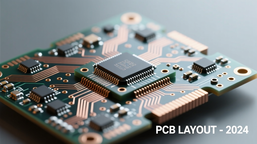
Ground Plane Splitting Pitfalls in Mixed-Signal PCBs: Real C
Analyze 3 documented EMI failures caused by improper ground plane segmentation—showing current return path disruption, noise coupling mechanisms, and corrected
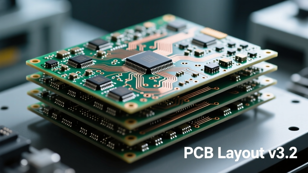
Controlled Depth Drilling Tolerances: When to Specify Back-D
Clarify fabrication feasibility thresholds—depth tolerance ±0.05mm vs. ±0.1mm—and decision logic for back-drilling vs. blind/microvias based on signal frequency
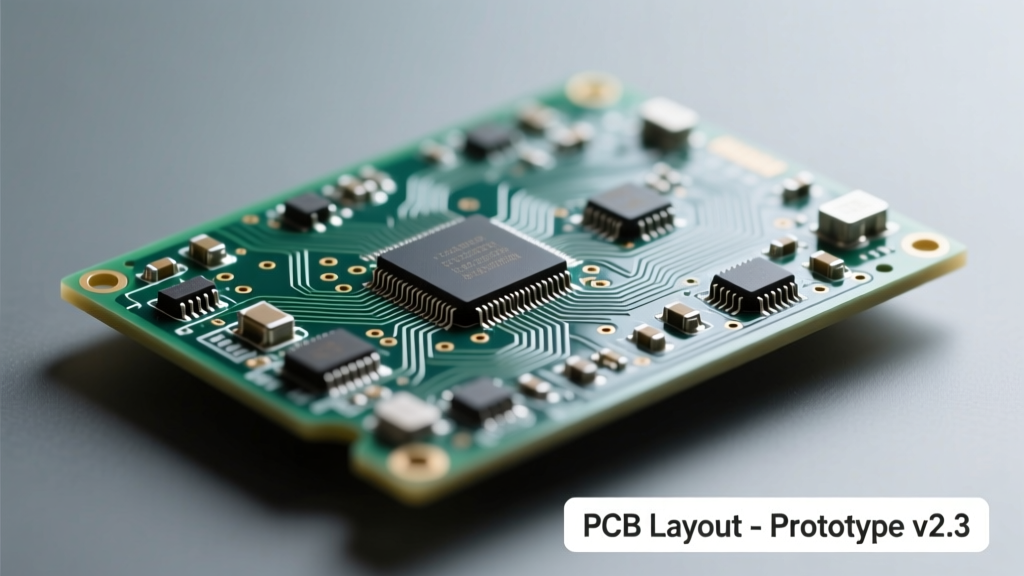
PCB Warpage Measurement Protocol: IPC-TM-650 2.4.22 Explaine
Break down the exact equipment setup, sample prep, temperature ramp profile, and pass/fail criteria from IPC-TM-650 2.4.22 for warpage testing—tailored for QA l
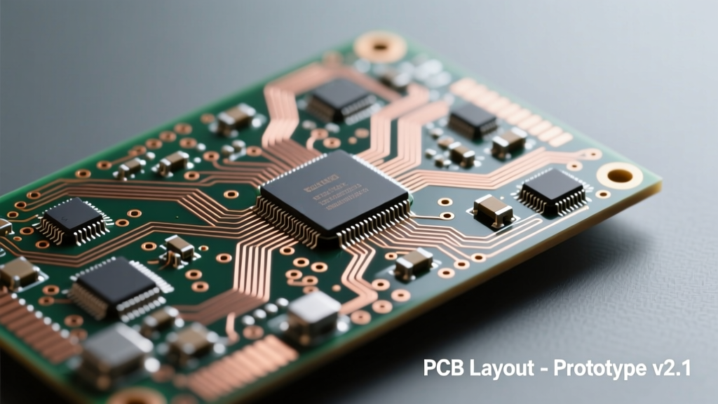
How to Design for Assembly (DFA) in Rigid-Flex PCBs: SMT Pad
Detail SMT pad geometry adjustments (length, soldermask dams, fiducial placement) required at rigid-to-flex transitions to prevent tombstoning and voiding durin
Thermal Relief Optimization for High-Current PCB Pads: 10A–1
Define minimum spoke count, width, and gap values for thermal reliefs under high-current pads (10A–100A), validated against IR thermography and voltage drop mea
Choosing Between Polyimide and LCP for High-Frequency Flex P
Compare dielectric constant stability, moisture absorption, loss tangent up to 40 GHz, and solder mask adhesion performance of polyimide vs. LCP substrates for
How to Validate Impedance Control on Multi-Dielectric PCBs
Walk through step-by-step impedance validation for boards with mixed dielectrics (e.g., FR-4 + Rogers), covering stackup modeling, TDR probe calibration, and cr
Rigid-Flex Stackup Comparison: 4-Layer vs. 6-Layer Reliabili
Compare real-world flex-cycle durability, impedance stability, and assembly yield between 4-layer and 6-layer rigid-flex designs using IPC-6013C test data and f
Thermal Via Placement Guide: Density, Size & Stackup Rules
Provide engineering-grade thermal via design rules—minimum/maximum spacing, optimal diameter-to-depth ratios, and layer-specific placement strategies for 4–12 l
Flex PCB Bending Radius Calculator: IPC-2223C Compliance Tab
Deliver a practical, downloadable bending radius reference table aligned with IPC-2223C Annex B, including copper thickness, coverlay type, and dynamic vs. stat
PCB Fabrication Tolerance Cheat Sheet: Cu Thickness to Etch
Map common base copper weights (½ oz to 3 oz) to recommended trace width compensation values per fab house capability tiers (standard, advanced, HDI), with etch
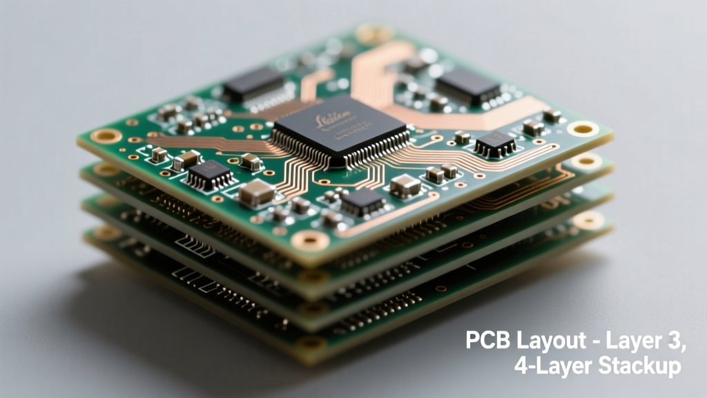
PCB Material Selection Matrix: FR-4 vs. High-Frequency Lamin
Compare Dk/Df stability, moisture absorption, and loss tangent across temperature/humidity for PAM4 eye opening at 28 GBd with real channel simulations.
Signal Integrity Checklist for High-Speed PCB Layouts
List and explain 12 actionable signal integrity verification steps engineers must perform before finalizing high-speed PCB layouts, including simulation validat
Design for Testability (DFT) in High-Speed PCBs: Probe Pad P
Specify probe pad size, clearance, reference plane access, and signal isolation requirements for boundary scan and high-speed oscilloscope probing.
Thermal Relief for High-Current Pads: When to Skip It (and R
Quantify thermal stress on pads carrying >10A during reflow using FEA models, defining current thresholds where thermal reliefs must be eliminated.
PCB Trace Width Calculator for Thermal Rise: 2°C vs. 10°C De
Explain IPC-2152-based trace width selection with real-world derating factors (solder mask, ambient airflow, adjacent traces) for precision thermal design.
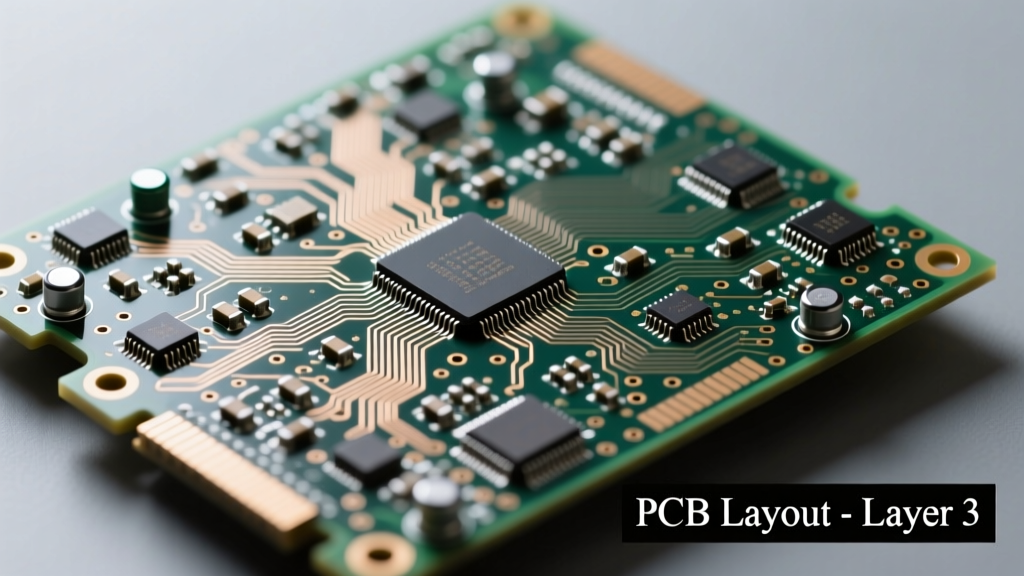
RF Grounding Best Practices: Via Fence Spacing, Stub Length
Define maximum via fence spacing relative to λ/20, stub resonance avoidance for RF switches, and integrated choke structures for LTE/WiFi bands.
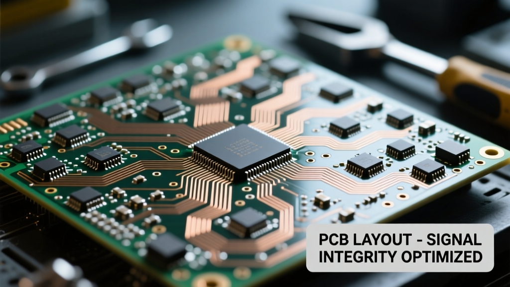
EMI Shielding Enclosures: PCB Layout Rules for Effective Far
Specify keep-out zones, gasket contact points, via fence spacing, and grounding strap placement aligned with IEC 61000-4-3 test standards.
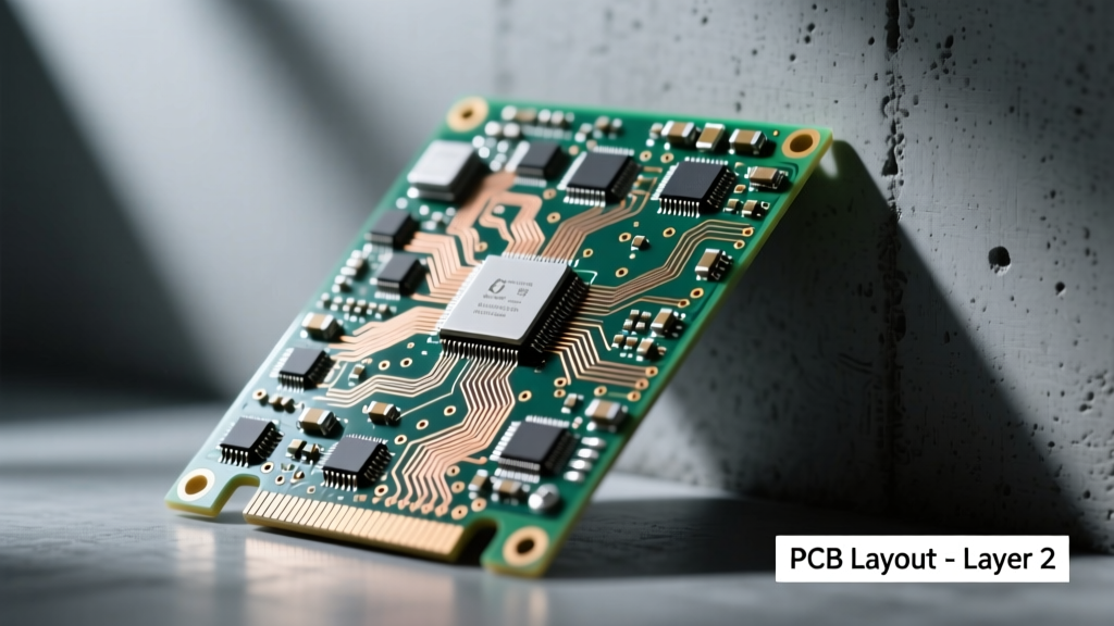
Via Transition Design: Reducing Insertion Loss in 28 Gbps Ch
Detail optimized anti-pad sizing, back-drill depth tolerances, and sequential build-up strategies for minimizing via transition loss above 14 GHz.
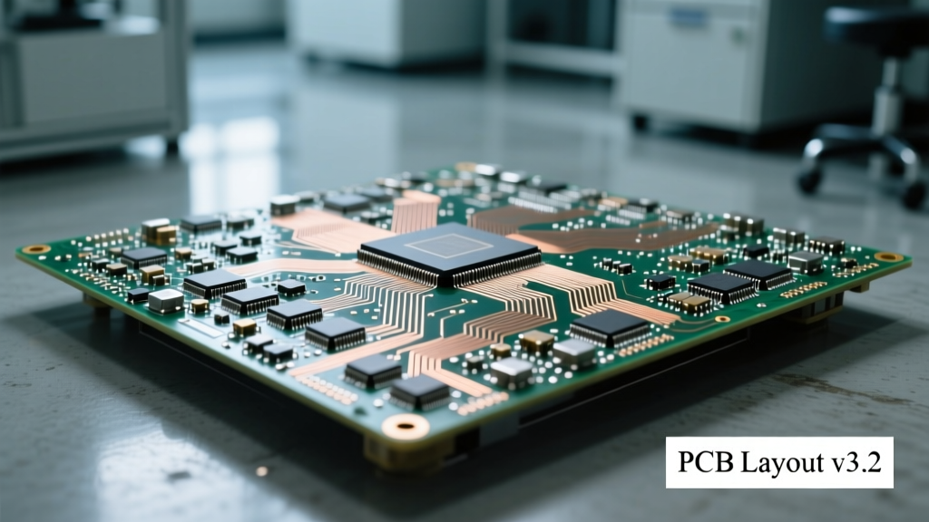
Controlled Impedance Routing for Flex PCBs: Bend Radius & Dy
Address impedance drift in dynamic flex areas with material-specific bend radius tables, copper thickness adjustments, and dynamic fatigue testing data.
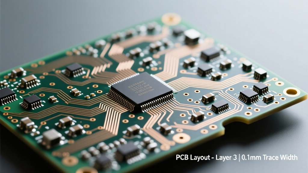
Return Path Design for High-Frequency Signals: Ground Plane
Illustrate return current distribution using EM simulators, specifying minimum ground plane width, cutout avoidance zones, and stitching via placement.
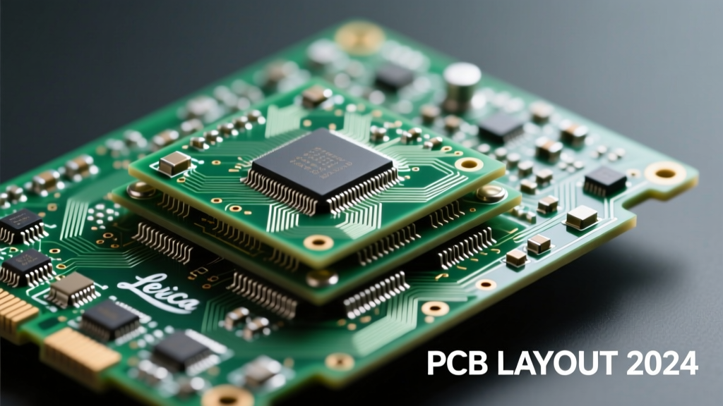
Stackup-Driven Signal Routing: How Layer Assignment Affects
Demonstrate crosstalk reduction by layer assignment (e.g., routing differential pairs between ground planes) with 3D EM simulation results.
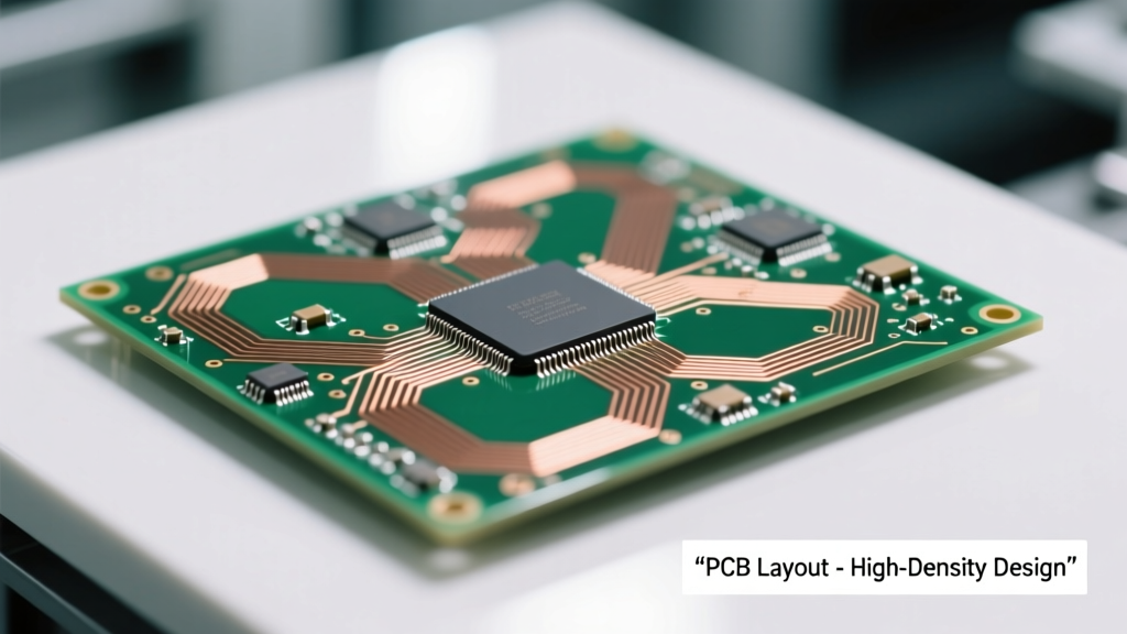
Capacitor Selection for PDN Decoupling: ESL vs. ESR Trade-Of
Compare ceramic, polymer, and embedded capacitors using impedance vs. frequency curves and show optimal placement distances from ICs.
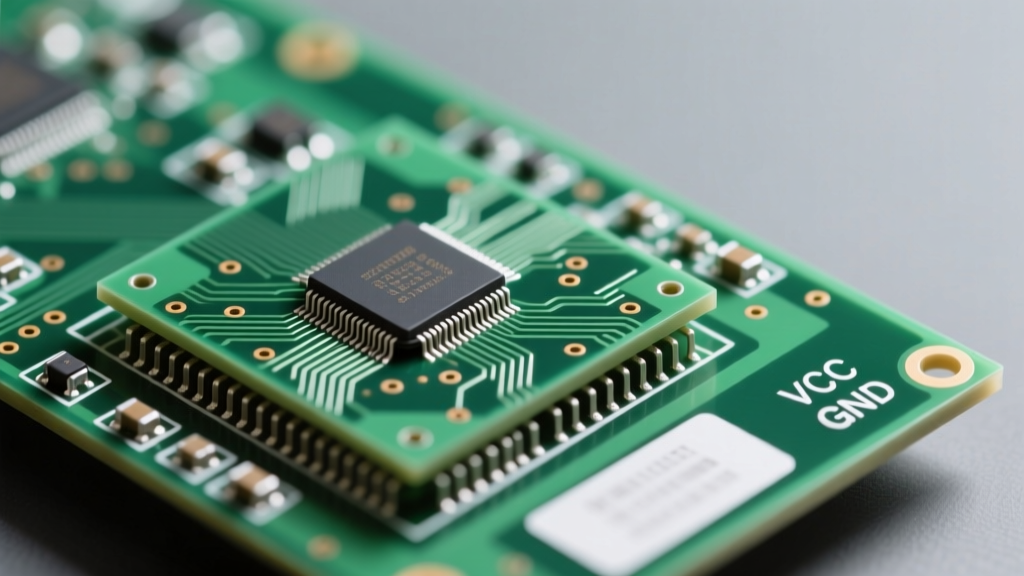
PCB Fabrication Notes That Prevent SI Failures: What to Spec
List 10 non-negotiable fabrication notes—e.g., copper roughness max, dielectric tolerance, solder mask thickness—for high-speed board quotes.