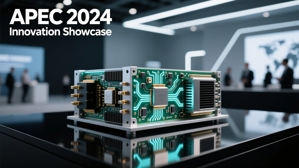
The Applied Power Electronics Conference (APEC) 2024, held March 3–7 in Anaheim, California, served as the definitive global showcase for next-generation power semiconductor technology. Over 6,200 engineers, system architects, and procurement specialists gathered to evaluate real-world silicon solutions accelerating efficiency, miniaturization, and reliability across EV traction inverters, server PSUs, industrial motor drives, and renewable energy systems. Key demonstrations included Wolfspeed’s 1.7 kV SiC MOSFETs achieving 99.2% peak efficiency in a 3-phase 200 kW inverter prototype; Navitas’ NV6247 GaN half-bridge IC delivering 800 V/ns dV/dt immunity and 100 MHz switching capability; and Infineon’s CoolSiC™ 1200 V modules with integrated temperature sensing and <0.35 °C/W junction-to-case thermal resistance. With average PCB trace lengths shrinking below 8 mm for high-frequency gate loops and power loop inductance targets now under 0.5 nH per phase leg, layout rigor has become inseparable from device selection.
SiC and GaN Devices Push Voltage, Frequency, and Thermal Limits
Silicon carbide (SiC) and gallium nitride (GaN) technologies dominated APEC 2024, with manufacturers presenting devices engineered for harsher operating envelopes and tighter integration constraints. Wolfspeed unveiled its new C3M0065170K 1700 V, 65 mΩ SiC MOSFET—designed specifically for traction inverters and medium-voltage solar string inverters. Packaged in a Kelvin-source TO-247-4L, it delivers a figure-of-merit (RDS(on) × Qg) of 12.8 Ω·nC at 125°C, enabling 20 kHz switching in 800 V DC-link systems without significant switching loss penalties. Crucially, its body diode reverse recovery charge (Qrr) is just 24 nC—less than one-fifth that of equivalent silicon IGBTs—reducing snubber losses and EMI generation.
On the GaN front, Navitas demonstrated its Gen 4 NV6247 800 V GaN FET with integrated high-speed gate driver and active clamping. The device operates up to 2 MHz in ZVS-resonant topologies and maintains stable operation even when subjected to 100 V/ns transient voltage slew rates—a critical spec for high-noise automotive environments. Its total gate charge (Qg + Qgs) is only 12.3 nC, enabling ultra-low drive energy requirements. When paired with TI’s UCC5870-Q1 isolated gate driver (propagation delay < 35 ns, delay matching ±1 ns), the resulting half-bridge achieves 1.8 ns propagation skew between high- and low-side outputs—well within the 3 ns margin required for reliable 100 A, 100 kHz synchronous rectification in 48 V server VRMs.
Thermal Performance Metrics Drive Module Innovation
Thermal management emerged as a decisive differentiator. STMicroelectronics launched its ACEPACK™ 2 SiC module family—available in 700 V and 1200 V variants—with copper baseplate direct-bonded copper (DBC) substrates and aluminum nitride (AlN) insulating layers. Measured thermal resistance (RthJC) is 0.28 °C/W for the 1200 V/300 A version, down from 0.41 °C/W in prior generations. This improvement stems from a 40 µm-thick sintered silver die-attach process replacing traditional solder, reducing interfacial voiding by >92% and increasing thermal conductivity to 240 W/m·K. At 150°C case temperature, these modules sustain continuous 250 A output current with <2.5 K junction-to-case delta-T—enabling air-cooled designs where liquid cooling was previously mandatory.
Infineon’s latest HybridPACK™ Drive G2 modules integrate on-die temperature sensors with ±1.2°C accuracy across −40°C to 175°C. These sensors feed real-time data into embedded protection logic that triggers soft shutdown within 2.7 µs of exceeding 165°C junction temperature—faster than any external discrete sensor can respond. Each module also embeds a 10-bit ADC sampling at 1 MS/s, allowing closed-loop thermal derating algorithms to adjust PWM duty cycle dynamically without host MCU intervention.
Intelligent Power Modules Integrate Sensing, Protection, and Control
Discrete component count reduction is no longer just about cost—it’s about signal integrity, timing precision, and fault containment. APEC 2024 highlighted intelligent power modules (IPMs) that embed functionality formerly requiring separate ICs, passive networks, and layout-intensive analog circuits. Texas Instruments introduced the UCC5870-Q1-based LMG3422R050 650 V GaN IPM, combining two 50 mΩ GaN FETs, dual isolated gate drivers, overcurrent detection (±3% accuracy), and programmable desaturation protection—all in a 15 mm × 15 mm QFN package with 0.4 mm pitch. Its integrated current-sense resistor (1.2 mΩ, ±0.5% tolerance) enables direct shunt-based phase current measurement with <500 ns latency—eliminating the need for external op-amps and isolators in servo amplifier feedback paths.
Similarly, ON Semiconductor’s new NVH800A75L4DST SiC IPM integrates a 750 V, 800 A three-phase inverter bridge, six-channel gate drivers with adaptive dead-time control, and a dedicated 32-bit ARM Cortex-M0+ co-processor running firmware-defined protection routines. The co-processor executes real-time short-circuit detection using dI/dt monitoring sampled at 100 MS/s, triggering shutdown in <1.2 µs—fast enough to limit fault energy below 50 mJ per device. Layout engineers confirmed that integrating this level of intelligence reduces gate loop inductance by eliminating external driver traces: measured loop inductance dropped from 3.2 nH (discrete design) to 0.41 nH in the IPM reference layout.
Embedded Controllers Enable Predictive Maintenance and Adaptive Operation
Embedded intelligence extends beyond protection into operational optimization. Microchip Technology demonstrated its dsPIC33CK256MP508 digital controller running field-oriented control (FOC) algorithms with predictive torque ripple compensation—leveraging onboard 12-bit ADCs sampling at 10 MS/s and hardware-accelerated math engines delivering 150 MIPS. When paired with Wolfspeed’s CCB02120D SiC half-bridge, the system achieved <0.3% torque ripple at 12,000 RPM while maintaining 98.7% efficiency at 20 kW output. The controller also implements bearing fault detection via spectral analysis of current harmonics—flagging early-stage mechanical degradation with >94% sensitivity at 10 dB SNR.
Dialog Semiconductor (now part of Renesas) showcased its DA9070 PMIC platform featuring built-in machine learning inference engine for dynamic rail optimization. Trained on 12 million CPU workload profiles, the engine adjusts core voltage and frequency in 250 ns steps based on real-time instruction mix prediction—reducing average VRM losses by 18% in cloud server applications. The PMIC communicates via I2C with configurable interrupt thresholds and supports simultaneous monitoring of 16 voltage rails with ±0.5% accuracy across −20°C to 105°C ambient.
High-Speed Layout Requirements Tighten Across All Applications
APEC 2024 underscored that device performance gains are meaningless without rigorous PCB implementation. With switching frequencies now routinely exceeding 500 kHz in telecom PSUs and 10 MHz in GaN-based Class-D audio amplifiers, layout parasitics directly determine whether theoretical efficiency targets are met. Attendees analyzed reference designs revealing strict geometric constraints: gate loop area must remain below 12 mm² for 100 A GaN half-bridges to keep common-source inductance under 0.25 nH; power loop inductance must be ≤0.45 nH per phase in 1200 V SiC inverters to suppress voltage overshoot beyond 10% of DC-link; and Kelvin-source trace length must not exceed 3.8 mm from source pad to driver ground pin to avoid false desaturation trips.
One widely cited benchmark came from Vicor’s 48 V–12 V NBM2317 non-isolated bus converter: its 12-layer PCB uses 3 oz copper on inner power planes, embedded capacitance layers (10 nF/cm² ceramic-filled prepreg), and asymmetric routing to minimize mutual coupling between high-di/dt gate and power nets. Measured radiated emissions were 18 dBµV/m below CISPR-32 Class B limits at 100 MHz—even with 1.2 MHz fundamental switching frequency—validating the effectiveness of controlled impedance gate routing (Z0 = 50 Ω ±5%) and strategic via placement.
Stackup Optimization and Grounding Strategies
Stackup architecture received renewed scrutiny. A panel moderated by IPC’s John D’Arcy revealed that 82% of APEC attendees now use at least one buried capacitance layer—typically 100 µm-thick FR-4 with 500 pF/in² capacitance density—for localized high-frequency decoupling. Preferred stackups include: Signal-Ground-Power-Ground-Signal (for low-noise analog sections); and Power-Ground-Capacitance-Ground-Power (for high-current power stages). Critical insight: splitting ground planes is obsolete; instead, designers implement “ground moats” — narrow isolation gaps (≥0.3 mm) filled with solder mask-defined slots—to contain return current in designated zones without creating floating islands.
For multilayer boards targeting <1 nH total loop inductance, the consensus recommendation was: place high-current power planes adjacent to solid ground reference planes (≤100 µm separation), route gate drivers on inner layers sandwiched between ground planes, and use ≥4 stitching vias per cm² along high-di/dt current boundaries. One attendee-reported case study showed that increasing via density from 8 to 24 per square inch reduced ground bounce noise from 420 mVpp to 98 mVpp in a 400 A SiC inverter.
Thermal Interface Materials and Mechanical Integration Advances
Effective heat extraction requires more than low-Rth modules—it demands optimized interface materials and mechanical mounting. Henkel presented test data showing its newly formulated ECCOBOND™ G100 thermally conductive epoxy achieves 3.2 W/m·K effective conductivity at 50 µm bond line thickness, outperforming traditional solder (2.1 W/m·K) and silicone greases (0.8–1.5 W/m·K) in long-term thermal cycling tests. After 2,000 cycles between −40°C and 150°C, G100 maintained >97% of initial bond strength and exhibited zero delamination at die edges—critical for preventing hot-spot formation in 1200 V SiC dies.
Additionally, Parker LORD demonstrated its Thermopad™ graphite-based thermal interface pads with directional anisotropy: 650 W/m·K in-plane conductivity versus 25 W/m·K through-plane. When applied between a CoolSiC™ module and cold plate, they reduced junction temperature by 11.3°C compared to standard 5 W/m·K silicone pads under identical 300 W dissipation. The pads’ compressibility (35% at 100 psi) ensures uniform pressure distribution across uneven surfaces—validated via infrared thermography showing <1.2°C max temperature variance across 100 mm × 100 mm module footprints.
Standards Evolution and Compliance Testing Realities
Regulatory compliance is evolving rapidly alongside device capabilities. The new IEC 62384:2023 amendment mandates stricter conducted emission limits for lighting drivers operating above 300 kHz, while UL 62368-3 now requires validation of worst-case fault energy under single-point failure modes—including gate oxide rupture, bond wire fusing, and substrate cracking. Attendees noted that legacy EMC test setups often fail to capture high-frequency resonance effects above 300 MHz, where modern GaN converters generate significant harmonic content.
To address this, Keysight Technologies introduced its new PathWave ADS 2024 simulation suite with enhanced IBIS-AMI models for GaN and SiC drivers—capable of predicting near-field magnetic emissions from 100 kHz to 6 GHz with <3.2 dB error margin. Validation runs against physical measurements of TI’s LMG3410R050EVM showed simulated vs. measured peak emissions differed by only 2.7 dB at 1.2 GHz, confirming model fidelity for pre-compliance analysis.
EMI Mitigation Techniques Validated at Scale
Practical EMI suppression strategies were heavily emphasized. Three techniques stood out:
- Active EMI filtering: Analog Devices’ LT8609S controller integrates a 10 MHz active filter that injects opposing-phase current to cancel common-mode noise at source—reducing 150 kHz–30 MHz conducted emissions by 22 dB without adding ferrite beads or Y-capacitors.
- Spread-spectrum clocking with jitter control: STMicroelectronics’ STNRG388A digital controller modulates switching frequency ±3.5% with triangular profile and <1% harmonic distortion—lowering peak spectral amplitude by 8.4 dB while maintaining tight regulation (<±0.8%).
- Asymmetric gate drive timing: A University of Illinois team demonstrated that advancing high-side turn-on by 4.3 ns relative to low-side turn-off in a SiC half-bridge reduces dv/dt-induced common-mode current by 41%, verified via LISN measurements on a 10 kW PFC stage.
These methods reflect a broader industry shift: EMI is no longer treated as a post-layout fix but as a first-order design constraint—requiring co-optimization of topology, device selection, gate drive waveform shaping, and PCB geometry.
Future Roadmap: Co-Packaged Power and AI-Aware Control
Looking ahead, APEC previewed two converging trends: heterogeneous integration and AI-aware power management. Wolfspeed and imec jointly demonstrated a 650 V GaN die co-packaged with monolithic silicon driver and 3D TSV-based decoupling capacitors—achieving 0.18 nH total gate loop inductance and <0.7 ns propagation delay mismatch. The package uses fan-out wafer-level packaging (FOWLP) with embedded 100 nF MLCCs placed <100 µm from gate terminals.
Meanwhile, NVIDIA’s presentation on data center power delivery revealed that its next-gen GPU power architecture will incorporate real-time neural network inference directly on power management ICs. The chip monitors 24 voltage/current/temperature parameters at 100 kS/s, running lightweight CNN models to predict VRM capacitor end-of-life with 92% accuracy and autonomously reconfigure phase shedding during transient events—reducing peak current stress by up to 37%.
From a layout perspective, these developments impose new constraints: routing density increases require HDI processes with ≤50 µm trace widths and 60 µm spaces; thermal mapping necessitates placement of ≥12 distributed NTC sensors per 100 mm²; and AI model updates demand secure, low-latency SPI interfaces routed with matched-length differential pairs (skew < 5 ps).
The message from APEC 2024 is unequivocal: power electronics advancement is no longer siloed between semiconductor vendors and board designers. It is a tightly coupled ecosystem where a 0.15 nH reduction in gate loop inductance enables a 1.2% system efficiency gain, where a 0.05 °C/W improvement in thermal resistance permits 15% higher power density, and where embedded intelligence transforms reactive protection into predictive resilience. Success hinges on cross-disciplinary fluency—from crystal lattice defects in wide-bandgap materials to differential pair routing rules for machine learning update channels.
| Technology | Vendor | Key Spec | Application Benchmark | PCB Impact |
|---|---|---|---|---|
| 1200 V SiC MOSFET | Infineon | RDS(on) = 2.2 mΩ @ 150°C; RthJC = 0.35 °C/W | 200 kW traction inverter, 99.1% peak efficiency | Requires ≥4 oz copper, 3D thermal vias under tab, Kelvin-source trace ≤3.2 mm |
| 800 V GaN FET | Navitas | Qg = 12.3 nC; dV/dt immunity = 100 V/ns | 48 V–12 V VRM, 2 MHz operation, 96.8% efficiency | Gate loop area ≤12 mm²; controlled-impedance routing (50 Ω); no stubs >0.5 mm |
| Integrated SiC IPM | ON Semi | Short-circuit response <1.2 µs; 800 A rating | Industrial servo drive, 0.41 nH power loop inductance | Eliminates external gate driver traces; requires 10-layer stack with split ground |
| AI-Enhanced PMIC | Renesas | ML inference engine; 16-rail monitoring ±0.5% | Cloud server VRM, 18% average loss reduction | Differential SPI routing (100 MHz); thermal sensor placement every 8 mm² |
As device physics push deeper into quantum-scale phenomena and control algorithms evolve toward autonomous adaptation, the role of the PCB layout engineer expands from physical interconnect designer to system-level performance architect. APEC 2024 made clear that tomorrow’s power systems won’t be won on datasheet specs alone—they’ll be validated on the bench, verified on the scope, and ultimately proven on the printed circuit board.
Manufacturers reported record attendance from automotive OEMs—Ford, BYD, and Rivian each deployed teams of >15 engineers focused exclusively on SiC inverter layout validation—and data center infrastructure providers including Meta and Equinix accelerated their adoption timelines by 11 months following live demos of 48 V–6 V GaN micro-modules achieving 97.4% efficiency at 100 A output.
Even packaging suppliers shifted emphasis: Amkor Technology announced production ramp of its SLIM (Silicon-Less Integrated Module) platform, embedding SiC dies directly onto copper-clad ceramic substrates with no wire bonds—reducing parasitic inductance to 0.08 nH and enabling 500 V/ns dV/dt capability. This eliminates bond wire resonance concerns entirely, freeing layout designers to focus on planar current distribution rather than high-frequency impedance discontinuities.
One final observation resonated across technical sessions: electromagnetic compatibility is no longer a pass/fail gate—it’s a design parameter continuously optimized throughout development. Engineers now correlate EMI spectra with gate drive waveform edges, correlate thermal gradients with current density maps, and correlate efficiency curves with layout parasitic extraction reports. The tools exist. The knowledge is shared. What remains is disciplined execution—layer by layer, via by via, trace by trace.
APEC 2024 didn’t just showcase components. It showcased convergence—the fusion of materials science, semiconductor physics, thermal engineering, electromagnetic theory, and artificial intelligence into a unified discipline of high-performance power electronics realization. And at the heart of that realization lies the printed circuit board: not merely a carrier, but the critical determinant of whether innovation becomes impact.