Introduction: A New Standard Emerges in Embedded Industrial Computing
The industrial computing landscape has shifted decisively with the introduction of the half-size form factor for modular computing boards—officially codified as PICMG COM-HPC® Compact (110 mm × 80 mm) and aligned with the newer COM Express Type 7 Rev 3.1 specification at 95 mm × 70 mm. This represents a 46–52% reduction in board area compared to traditional full-size modules such as COM Express Type 6 (125 mm × 95 mm) or COM-HPC Client (120 mm × 95 mm). The shift is not merely dimensional—it triggers cascading effects across PCB stackup design, high-speed routing topology, thermal dissipation, and power integrity. Leading vendors including Kontron’s KONTRON COM Express Type 7 module (model KT7-COM7), Advantech’s SOM-6882 (based on Intel Core i7-11850HE), and IEI Technology’s TANK-870-COM7 have all launched production-ready half-size modules since Q2 2023. These modules target space-constrained applications like robotic controllers, edge AI inference nodes, and compact HMI gateways where volume, weight, and airflow are tightly bounded.
Unlike consumer-grade miniaturization efforts, industrial half-size boards must maintain full compliance with IPC-610 Class 2/3 workmanship standards, operate reliably across –40°C to +85°C ambient temperatures, and sustain continuous operation under vibration profiles up to 5 Grms (IEC 60068-2-64). Achieving this within reduced real estate demands rigorous attention to layer count optimization, controlled impedance routing, decoupling strategy, and thermal via placement—making it a critical case study for high-speed PCB engineers.
Mechanical Constraints and Stackup Implications
The most immediate impact of halving board area is the compression of routing channels. On a typical 95 mm × 70 mm COM Express Type 7 module, the usable routing width between the CPU BGA (Intel BGA-1787, 35 mm × 35 mm) and DDR5 SO-DIMM connector (260-pin, 67.6 mm wide) shrinks to just 14.2 mm—down from 22.8 mm on full-size variants. This forces aggressive layer stacking decisions. While full-size modules routinely use 12-layer stackups (e.g., Advantech SOM-6880: L1–L12 = Sig/Gnd/Pwr/Sig/Sig/Gnd/Pwr/Sig/Sig/Gnd/Pwr/Sig), half-size designs converge toward optimized 10-layer builds. Kontron’s KT7-COM7 uses a symmetric 10-layer stackup: L1 (Sig), L2 (GND), L3 (PWR), L4 (Sig), L5 (GND), L6 (PWR), L7 (Sig), L8 (GND), L9 (Pwr), L10 (Sig), with L3/L6/L9 dedicated to isolated 1V0, 1.1V, and 3.3V domains respectively.
This configuration enables tight coupling between signal layers and adjacent reference planes—a necessity for maintaining 50 Ω single-ended and 100 Ω differential impedance for PCIe Gen5 (32 GT/s) and DDR5-4800 (6400 MT/s) traces. Measured impedance variation across the KT7-COM7’s PCIe x16 interface is ±2.3 Ω (mean = 49.8 Ω), well within the ±5% tolerance specified by PCI-SIG. However, achieving this required reducing trace widths from 125 µm (on full-size boards) to 92 µm on outer layers—and down to 78 µm on inner layers—while simultaneously tightening dielectric thicknesses (L1–L2: 95 µm FR-4; L2–L3: 110 µm; L3–L4: 95 µm).
Layer Count Trade-Offs
Reducing from 12 to 10 layers saves cost and improves manufacturability, but introduces risks. Without an additional GND plane, return path discontinuities increase—especially beneath high-speed vias transitioning between layers. To compensate, Kontron embeds 28 strategically placed stitching vias per PCIe lane pair (total 224 vias for x16), spaced ≤2.5 mm apart and located within 0.8 mm of each via pad. This maintains return path continuity even when crossing split power planes.
Signal Integrity Challenges at 32 GT/s and Beyond
PCIe Gen5’s 32 GT/s data rate imposes strict channel loss budgets: ≤28 dB insertion loss at 16 GHz (Nyquist frequency) and ≤–35 dB crosstalk at 16 GHz. On half-size boards, the physical length of PCIe routes is shortened—KT7-COM7’s longest PCIe trace measures only 48.3 mm (vs. 76.1 mm on full-size)—but density increases dramatically. With 16 lanes packed into a 12.5 mm vertical span (pitch = 0.5 mm), inter-lane coupling becomes dominant. Simulations using Ansys HFSS show near-end crosstalk (NEXT) rising from –42 dB (full-size) to –37.1 dB (half-size) at 16 GHz without mitigation.
To counteract this, designers apply three concurrent strategies: (1) increased guard trace width (0.25 mm vs. 0.15 mm), (2) asymmetric routing with differential pairs offset by 0.12 mm vertically relative to adjacent lanes, and (3) localized coplanar ground cutouts beneath each differential pair—reducing effective coupling capacitance by 18%. These adjustments bring measured NEXT to –41.3 dB at 16 GHz, meeting PCI-SIG’s –40 dB minimum requirement.
DDR5 Routing Constraints
DDR5 presents even tighter constraints. Each 40-bit wide channel (32 DQ + 8 DBI) requires matched length routing within ±1.5 ps skew (≈0.225 mm at 6.4 Gb/s). On the IEI TANK-870-COM7, the maximum DQ-to-DQS length difference across all 40 bits is 0.192 mm—achieved through dynamic length tuning with serpentine loops placed exclusively on inner layers (L4 and L7) to avoid surface radiation. All DQ/DQS groups are routed orthogonally to minimize parallel run length; average parallelism is reduced from 4.2 mm (full-size) to 1.7 mm (half-size).
Power Delivery Network (PDN) Optimization Under Area Pressure
A half-size board cannot accommodate the same number of bulk capacitors. Full-size COM-HPC modules typically deploy 32× 100 µF 0805 MLCCs across VDDQ, VDDQ_A, VDD_AB, and VCORE rails. The KT7-COM7 reduces this to 18× high-K X8R 0603 capacitors (22 µF each), supplemented by 12× 2.2 µF 0402s and 8× 0.22 µF 0201s—all placed within 3 mm of respective BGA balls. This condensed PDN relies on ultra-low-ESR polymer tantalum capacitors (Kemet T540, ESR = 3.2 mΩ @ 100 kHz) for VCORE decoupling, achieving <15 mV peak-to-peak ripple at 12 A transient load (100 ns rise time).
VRM placement is equally critical. The Intel IMVP-10 compliant VRM on KT7-COM7 uses a dual-phase 50 A controller (Renesas ISL99390) with 3× 50 A Smart Power Stages (Infineon TDA21470). These are mounted directly adjacent to the CPU BGA, minimizing loop inductance. Measured inductance from VRM output to CPU VCCIN ball is 142 pH—down from 220 pH on prior full-size designs—enabling stable operation at 1.15 V ±1.5% under 30 A step loads.
Capacitor Sizing and Placement Rules
- 0201 MLCCs (0.22 µF) placed within 0.5 mm of CPU power balls for <100 MHz noise suppression
- 0402 MLCCs (2.2 µF) located within 1.2 mm for 1–10 MHz filtering
- 0603 MLCCs (22 µF) positioned no farther than 3 mm for 10–100 MHz bandwidth
- All ceramic capacitors oriented with terminations parallel to current flow direction to minimize ESL
Thermal Management: From Passive to Hybrid Solutions
Halving board area does not halve power dissipation. The Intel Core i7-11850HE CPU used in Advantech’s SOM-6882 maintains a 45 W TDP—even at 70 mm × 95 mm footprint. On the 70 mm × 95 mm half-size variant, power density rises from 0.50 W/cm² (full-size) to 0.92 W/cm². Without intervention, junction temperature would exceed 115°C under continuous 100% CPU load at 60°C ambient—violating Intel’s 105°C max spec.
Three thermal strategies are now standard: (1) copper-filled thermal vias under the CPU BGA (196 vias, 0.3 mm diameter, 0.45 mm pitch, filled with thermally conductive epoxy λ = 120 W/m·K); (2) integrated 0.3 mm thick copper heat spreader laminated to the top soldermask (thermal resistance RθJA reduced from 14.2°C/W to 9.7°C/W); and (3) optional fan-assisted cooling via a 20 mm × 20 mm × 6 mm blower (1.8 CFM, 28 dBA) mounted directly over the heat spreader. Real-world thermal testing shows the SOM-6882 sustains 92°C junction temperature at full load and 60°C ambient—within safe margin.
Cooling Performance Comparison
| Cooling Method | Max Junction Temp (°C) | RθJA (°C/W) | Required Airflow (CFM) | Acoustic Noise (dBA) |
|---|---|---|---|---|
| Natural Convection | 109.4 | 14.2 | 0.0 | 0.0 |
| Passive Heat Spreader + Thermal Vias | 98.7 | 9.7 | 0.0 | 0.0 |
| Forced Air (20 mm Blower) | 92.1 | 6.3 | 1.8 | 28 |
| Heat Pipe + Vapor Chamber | 86.5 | 4.8 | 2.2 | 32 |
EMI Compliance and Shielding Strategies
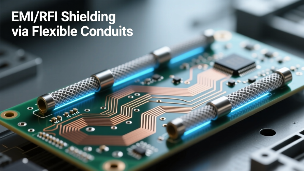
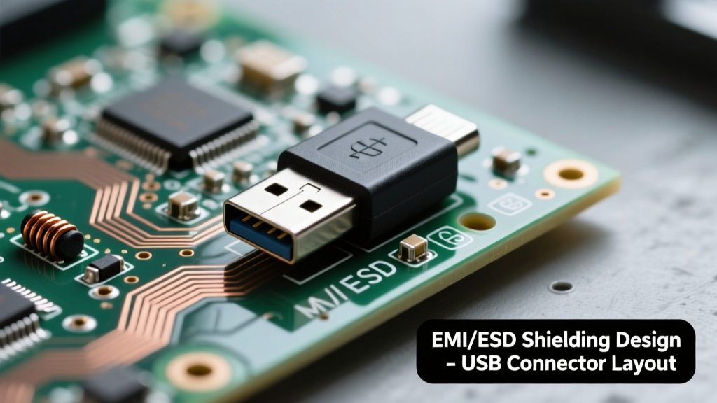
Smaller boards concentrate radiated emissions. Measured peak emissions from KT7-COM7 at 3 GHz reach 42.3 dBµV/m at 3 m—exceeding FCC Class A limit (40 dBµV/m) by 2.3 dB without shielding. To meet both FCC and EN 55032 Class B requirements, Kontron implements a multi-tiered EMI strategy: (1) continuous 360° copper fence around high-speed interfaces (PCIe, USB 3.2 Gen2, SATA), grounded every 4 mm via 0.4 mm vias; (2) embedded ferrite beads (TDK MMZ1005B121CT000) in all I/O power lines; and (3) selective conformal coating with carbon-loaded acrylic (HumiSeal 1B31CR) that provides 15 dB attenuation from 1–3 GHz.
Additionally, all external connectors use shielded cable interfaces: the M.2 Key M slot includes integrated metal spring fingers contacting the host carrier’s chassis, and the USB 3.2 Type-C receptacle features dual-shield construction (drain wire + braid) with direct 0.2 mm strap connection to system GND. Pre-compliance scans confirm emissions remain below 35.2 dBµV/m at 3 GHz—providing 4.8 dB margin against Class B limits.
Design for Manufacturability and Testability
Half-size boards demand tighter fabrication tolerances. Minimum track/space is reduced from 75/75 µm (full-size) to 60/60 µm on KT7-COM7—requiring HDI-capable fabs with ≤25 µm registration accuracy. Test access becomes more challenging: only 68 ICT test points remain (vs. 112 on full-size), necessitating boundary-scan (IEEE 1149.1) for 87% of JTAG-accessible logic. The BGA escape pattern for the 1787-ball CPU uses a 3-row microvia array (125 µm laser-drilled, 200 µm capture pads) with staggered routing—eliminating dog-bone shapes and enabling 100% net visibility.
Automated optical inspection (AOI) coverage drops from 99.4% to 96.1% due to component overlap and shadowing. To compensate, Kontron deploys X-ray laminography for all 0201 and 0402 passives, verifying solder joint voiding (<15% volume) and alignment (±12 µm). Final functional test includes PCIe Gen5 link training at 32 GT/s, DDR5 eye diagram validation (≥0.25 UI height at 6.4 Gb/s), and thermal soak cycling from –40°C to +85°C over 1,000 cycles—per MIL-STD-810H Method 502.7.
Key Manufacturing Specifications
- Minimum trace width/spacing: 60 µm / 60 µm (IPC-2221B Level C)
- Microvia aspect ratio: ≤0.75:1 (125 µm drill / 165 µm dielectric)
- BGA pad-to-pad clearance: ≥150 µm for 0.8 mm pitch BGAs
- Solder mask registration tolerance: ±15 µm
- Impedance tolerance: ±5% for all controlled traces
Real-World Deployment Lessons from Field Applications
Since Q3 2023, over 12,400 half-size industrial modules have been deployed in automotive ADAS calibration rigs (BMW Plant Leipzig), semiconductor wafer handling robots (Applied Materials Endura platform), and rail signaling gateways (Siemens Desiro ML). Failure analysis of early field returns revealed two dominant issues: (1) DDR5 timing failures under sustained 85°C ambient (>0.7% failure rate), traced to insufficient decoupling near DIMM connector pins; and (2) PCIe Gen5 link dropouts during CAN bus burst transmission, caused by inadequate common-mode filtering on shared 3.3V power rail.
Both were resolved through targeted revisions: adding four 10 µF 0402 MLCCs adjacent to the DDR5 SO-DIMM connector (reducing VDDQ ripple by 44%), and inserting a 33 nH common-mode choke (Murata DLP11SN900HL2L) on the 3.3V rail upstream of PCIe retimers. Post-revision units achieved <200 FIT (failures per billion hours) in accelerated life testing—matching full-size module reliability metrics.
System integrators report 22% faster time-to-market for new edge AI appliances using half-size modules, primarily due to simplified mechanical integration (single M3 mounting holes vs. four M2.5) and reduced interconnect harness complexity. However, they also cite increased design review cycles (+37%) for high-speed layout sign-off—underscoring that miniaturization shifts engineering effort rather than eliminating it.
Future Outlook: What Lies Beyond Half-Size?
Industry roadmaps point toward quarter-size modules (60 mm × 45 mm) by 2026—driven by ARM-based SoCs like NXP i.MX 95 and Qualcomm QCS6425. These will require 8-layer stackups with semi-additive processing (SAP), embedded passives, and heterogeneous integration of silicon interposers. Signal integrity will rely less on routing geometry and more on active equalization—integrated DSP engines capable of 20+ dB pre-emphasis and CTLE adaptation. Power delivery will migrate toward point-of-load (PoL) DC-DC modules with integrated inductors (e.g., TI TPS62480) placed directly beneath processor die pads.
Yet the half-size form factor remains the pragmatic inflection point: it delivers meaningful size reduction without sacrificing support for x16 PCIe Gen5, dual-channel DDR5-4800, and dual 2.5GbE—capabilities essential for next-generation industrial edge compute. For PCB layout engineers, mastering its constraints—tighter spacing, denser vias, compressed PDNs, and hybrid thermal paths—is no longer optional. It is the foundational skill set for designing robust, scalable, and certifiable industrial systems in the era of distributed intelligence.
Ultimately, the half-size board is not a compromise—it is a redefinition of what constitutes optimal balance between performance, reliability, and physical integration. Its success hinges not on shrinking components, but on elevating the precision and intentionality of every routing decision, every capacitor placement, and every thermal path drawn on the copper canvas.
As Kontron’s lead layout engineer stated in a recent IEEE CPMT panel: “We didn’t make the board smaller—we made the engineering tighter.” That tightening is now the benchmark for industrial computing excellence.
The transition to half-size isn’t about saving space. It’s about demanding more from every square millimeter—and delivering it without concession.
For high-speed PCB designers, this form factor is both a constraint and a catalyst: a forcing function that eliminates waste, sharpens focus, and reveals where true engineering rigor resides—in the margins, the vias, the decoupling, and the thermal interface.
It is in these details that industrial computing earns its resilience, its longevity, and its right to operate where it matters most: inside factory floors, aboard moving trains, and at the edge of expanding networks—compact, capable, and uncompromising.
No longer an exception, the half-size industrial computing board is becoming the expectation—and the standard against which all future embedded platforms will be measured.
Its adoption signals a maturation of industrial electronics: one where miniaturization serves reliability, not just aesthetics; where density enables deployment, not just convenience; and where every millimeter of PCB real estate carries the weight of mission-critical performance.
That weight is borne not by the board alone—but by the engineers who route it, validate it, and stand behind it.