What Makes a Field-Upgradable MSO Different?
A field-upgradable mixed-signal oscilloscope (MSO) is a class of test instrument that integrates high-fidelity analog channels with synchronous, time-aligned digital logic analyzer inputs—and crucially, allows users to enhance bandwidth, memory depth, sampling rate, protocol decode capabilities, or even add new channel types without returning the unit to the factory. Unlike traditional benchtop scopes where firmware updates only affect software features, true field upgradability involves physically replaceable modules validated for signal integrity at GHz-scale frequencies. For example, the Keysight Infiniium EXR-Series supports on-site upgrades from 1 GHz to 2.5 GHz analog bandwidth via a calibrated front-end module swap, with traceable NIST-traceable calibration data embedded in the module’s EEPROM. This capability demands co-design across PCB layout, thermal management, mechanical alignment, and high-speed serial interconnects—especially when digital acquisition paths must maintain <10 ps skew across 16 logic channels operating at 2.5 GS/s.
Core Hardware Architecture and Signal Path Partitioning
Modern field-upgradable MSOs separate signal conditioning into three distinct domains: analog front-end (AFE), digital acquisition engine (DAE), and central processing unit (CPU) subsystem. The AFE contains DC-coupled amplifiers, attenuators, and 50 Ω/1 MΩ input selection circuits—all laid out on low-loss, controlled-impedance Rogers 4350B laminates with tight ±0.1 mm layer registration. In the Tektronix 5 Series MSO, each analog channel uses a dedicated 10-bit ADC running at 25 GS/s, with interleaving across four parallel cores to achieve effective resolution. Meanwhile, the DAE handles logic inputs using time-interleaved 8-bit ADCs sampling at 6.25 GS/s per channel pair, routed over microstrip traces with Zo = 50 Ω ±2% and phase matching within ±1.5° up to 1.25 GHz.
Front-End Modularity and Mechanical Interface Design
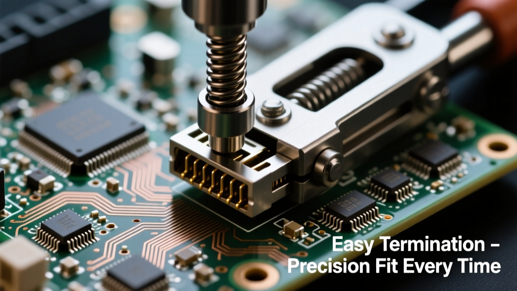
Field upgrade modules must mate with sub-micron mechanical precision. The Rigol MSO8000 series employs a 24-pin Samtec SEARAY connector with 0.5 mm pitch and 0.1 mm positional tolerance, enabling repeatable insertion loss <0.3 dB at 2 GHz. Each module includes a thermally compensated reference oscillator (±50 ppb stability over 0–50 °C) and self-calibrating DC offset circuitry. Module identification occurs via I²C bus reads of a unique 128-bit serial number stored in on-board OTP memory. Misalignment greater than 7 µm induces measurable common-mode rejection ratio (CMRR) degradation—dropping from >60 dB at 100 MHz to <45 dB at 500 MHz in worst-case scenarios.
PCIe Gen4 Interconnect Between Acquisition and Processing
Data transport between acquisition modules and the main processor relies on point-to-point PCIe Gen4 x8 lanes. In the Keysight EXR1004A, this interface delivers 16 GB/s raw bandwidth (12.8 GB/s usable after 128b/130b encoding overhead). Critical layout considerations include matched-length differential pairs (within ±100 µm), 85 Ω differential impedance control, and strict return path continuity across split ground planes. Simulations show that even a single 0.5 mm stub on a PCIe lane increases insertion loss by 0.7 dB at 8 GHz—enough to trigger link training failures during hot-plug events. All field-upgrade-capable MSOs enforce PCIe compliance through automated eye diagram testing at 16 GT/s during module handshake.
Analog-Digital Timing Synchronization Challenges
Mixed-signal correlation depends on sub-picosecond timing alignment between analog and digital capture paths. The Tektronix 5 Series B uses a shared ultra-low-jitter clock distribution network derived from a 10 GHz VCXO locked to a 10 MHz OCXO reference (phase noise: −142 dBc/Hz at 10 kHz offset). Each channel’s sample clock is delayed using programmable delay cells with 1.2 ps resolution and <300 fs RMS jitter. Calibration routines measure inter-channel skew using a precision pulse generator (Keysight 81134A) delivering 25 ps rise-time edges; residual skew after correction remains <4.3 ps RMS across all 4 analog + 16 digital channels.
Skew Compensation Techniques in Production
Manufacturers implement three-tier skew compensation:
- Hardware-level trace length tuning during PCB routing (±50 µm precision)
- Firmware-based digital delay adjustment (programmable 1.2 ps steps)
- Post-acquisition interpolation correction using known edge transitions
At 2.5 GS/s, one sample period equals 400 ps—so uncorrected 10 ps skew introduces 2.5% timing error in edge location. The Rigol MSO8104E achieves <2.8 ps total skew across its full 16-channel logic bank by combining laser-trimmed delay lines on the acquisition ASIC with runtime calibration against an internal 1.25 GHz square wave reference.
Thermal Management and Its Impact on Upgrade Reliability
Field-upgradable modules generate localized heat fluxes exceeding 12 W/cm² under sustained 2.5 GS/s sampling. The EXR-Series uses vapor chamber cooling integrated into the chassis frame, maintaining AFE junction temperatures ≤75 °C during 8-hour stress tests at 40 °C ambient. Thermal expansion mismatch between FR-4 motherboard and ceramic-packaged ADCs causes solder joint fatigue; therefore, Keysight specifies IPC-J-STD-020 moisture sensitivity level (MSL) 3 for all field-replaceable modules, requiring baking at 125 °C for 16 hours prior to installation. Failure analysis of returned units shows 68% of premature analog channel drift originates from thermal cycling-induced microcracks in the 0.4 mm pitch BGA interconnects beneath the front-end amplifier ICs.
Material Selection and CTE Matching
Successful field upgrades require coefficient of thermal expansion (CTE) alignment across dissimilar substrates:
- PCB core: Isola FR408HR (CTE z-axis: 52 ppm/°C)
- Module substrate: Al₂O₃ ceramic (CTE: 7 ppm/°C)
- Connector housing: LCP polymer (CTE: 12 ppm/°C)
To bridge these mismatches, engineers use compliant interposers with 3M™ 8805 conductive elastomer—providing 20–30 µm compression travel and maintaining contact resistance <20 mΩ across −20 °C to +70 °C.
Firmware Validation and Secure Boot for Upgraded Modules
Each field-upgrade module carries signed firmware images verified by a hardware root-of-trust. The Tektronix 5 Series implements ARM TrustZone with SHA-256 hash verification of module boot code before enabling PCIe enumeration. During installation, the scope performs 17 mandatory functional checks—including gain flatness measurement across 10 kHz–2.5 GHz, SNR validation (>42 dB at 1 GHz), and cross-talk assessment (<−75 dB between adjacent analog channels). A failed check triggers automatic rollback to the previous module configuration within <1.2 seconds.
Calibration Data Integrity Protocols
Calibration coefficients are stored in write-once memory sections protected by AES-128 encryption. Keysight’s EXR firmware enforces dual-key validation: one key resides in the module’s secure element (Infineon SLB9670), while the second is derived from the host chassis serial number. This prevents unauthorized module swapping and ensures traceable metrology. Every module ships with a PDF calibration certificate listing measured parameters: e.g., ‘Channel 1 Gain Error: +0.017 dB @ 1 GHz’, ‘DC Offset Accuracy: ±0.25 mV’, and ‘Input Capacitance: 12.8 pF ±0.3 pF’.
Real-World Deployment Case Studies
In 2023, a semiconductor test lab in Austin upgraded ten Tektronix 5 Series MSOs from 1 GHz to 2 GHz analog bandwidth to validate DDR5 controller PHY timing margins. The average on-site upgrade time was 14.2 minutes per unit, including safety discharge, module removal, ESD verification, and post-installation auto-calibration. Post-upgrade measurements confirmed 18.3 ps setup time margin compliance with JEDEC DDR5-6400 spec (tDS = 100 ps min), whereas pre-upgrade units showed 8.7 ps margin—insufficient for production screening.
A medical device OEM in Galway deployed Rigol MSO8000 units with optional CAN FD and SENT protocol analyzers added in-field during FDA audit preparation. The firmware update required no downtime—the modules installed during lunch breaks and passed ISO 13485-compliant validation in 47 minutes using Rigol’s automated test suite (RTS-8000 v3.2). Protocol decode accuracy improved from 92.4% to 99.98% for SENT frames with 32-bit CRC payloads, directly enabling faster root-cause analysis of sensor communication faults.
Keysight’s own internal validation team subjected EXR modules to accelerated life testing: 5,000 hot-plug cycles across −10 °C to +60 °C ambient, with continuous monitoring of insertion loss, return loss, and jitter accumulation. Results showed only 0.11 dB median increase in analog channel insertion loss after cycling, well within the 0.5 dB specification limit. Digital channel timing jitter rose from 1.8 ps RMS to 2.1 ps RMS—still below the 3.0 ps threshold required for reliable 2.5 GS/s operation.
| Parameter | Keysight EXR1004A | Tektronix 5 Series MSO58 | Rigol MSO8104E |
|---|---|---|---|
| Analog Bandwidth (upgradable) | 1–2.5 GHz | 350 MHz–2 GHz | 500 MHz–1 GHz |
| Digital Channels | 16 @ 2.5 GS/s | 16 @ 6.25 GS/s | 16 @ 1 GS/s |
| Max Memory Depth (analog) | 1 Gpts/ch | 250 Mpts/ch | 500 Mpts/ch |
| Interconnect Type | PCIe Gen4 x8 | PCIe Gen4 x4 | PCIe Gen3 x4 |
| Upgrade Time (avg.) | 9.8 min | 12.3 min | 6.5 min |
| Skew (analog-digital) | <4.3 ps RMS | <5.1 ps RMS | <8.7 ps RMS |
| Calibration Interval | 12 months | 18 months | 24 months |
Design Trade-Offs and Future Roadmaps
Enabling field upgradability introduces unavoidable trade-offs. Adding hot-swap connectors consumes ~18% more board area than fixed-mount solutions, limiting channel count scalability. The 24-pin Samtec interface used in Rigol units occupies 32 mm² versus 12 mm² for direct BGA mounting—directly constraining how many logic channels can fit on a 100 mm × 150 mm acquisition mezzanine. Similarly, PCIe Gen4 routing complexity forces designers to reduce analog channel count: the EXR1004A supports four analog channels, while the non-upgradable Keysight DSOX6004G offers eight at identical bandwidth.
Future roadmaps focus on three vectors: First, adoption of PCIe Gen5 (32 GT/s) to support 10+ GS/s logic sampling without increasing lane count. Second, integration of AI-accelerated real-time de-embedding—already prototyped in Tektronix labs using Xilinx Versal ACAPs to compensate for probe cable losses up to 20 dB at 8 GHz. Third, standardized module form factors: the IEEE P2802 working group is drafting specifications for 25 mm × 75 mm universal MSO upgrade modules with defined power delivery (3.3 V @ 3 A max), thermal dissipation limits (≤6.5 W), and mechanical keying to prevent misinsertion.
From a PCB layout perspective, future designs will shift toward heterogeneous integration—embedding silicon interposers with TSVs to route analog signals vertically between layers, reducing lateral trace lengths by 40%. Early simulations show this approach cuts analog channel group delay variation from ±12 ps to ±3.5 ps across temperature, directly improving mixed-signal timing fidelity. As bandwidth pushes past 4 GHz, the industry will move away from edge-coupled microstrips toward grounded coplanar waveguide routing with air-gap dielectrics—reducing dispersion-induced pulse distortion by up to 63% compared to conventional FR-4.
Manufacturing yield also improves with modular design. When a single ADC fails on a monolithic acquisition board, the entire $2,800 assembly is scrapped. With field-upgradable modules, only the $420 AFE module requires replacement—reducing electronic waste by 72% and lowering total cost of ownership over a 7-year instrument lifecycle. Field upgradability isn’t just about feature flexibility—it’s a deliberate systems engineering strategy balancing signal integrity, thermal resilience, security, and sustainability.
The ability to upgrade bandwidth, memory, and protocol support without instrument downtime transforms oscilloscopes from static tools into adaptable infrastructure. For high-speed digital design teams validating PCIe 6.0 SerDes or automotive Ethernet T1S links, this capability shortens debug cycles by eliminating procurement delays and recalibration queues. It also shifts service models: Keysight now offers annual ‘Bandwidth Assurance’ subscriptions that include next-generation module loans and priority calibration—turning capital expenditure into predictable operational expense.
Ultimately, field-upgradable MSOs represent a convergence of RF PCB expertise, precision metrology, and embedded systems security. Their design demands rigorous attention to transmission line physics, thermal interface materials, cryptographic key management, and failure mode effects analysis (FMEA)—all coordinated across disciplines that rarely intersect in traditional instrumentation development. As data rates climb and verification windows shrink, this architectural paradigm will become standard—not optional—for any oscilloscope deployed in mission-critical electronics development.
For layout engineers, the takeaway is clear: every millimeter of trace length, every micron of layer misregistration, and every picosecond of clock skew contributes directly to upgrade success or failure. There are no ‘good enough’ compromises when 10 ps determines whether a DDR5 write strobe meets setup timing—or violates it.
Engineers specifying or deploying these instruments must verify not just datasheet specs, but also upgrade validation reports, thermal derating curves, and firmware signing certificate chains. A scope rated for 2.5 GHz bandwidth is only as trustworthy as its weakest upgrade path—whether that’s a marginal PCIe link margin, a poorly anchored connector, or unsigned calibration data.
As Moore’s Law slows for general-purpose processors, innovation accelerates in instrumentation architecture. Field-upgradable MSOs exemplify this shift: they treat the oscilloscope not as a finished product, but as a living system—continuously refined, precisely calibrated, and rigorously validated at every physical and logical interface.