What Is a Programmable Op Amp—and Why It Matters Now
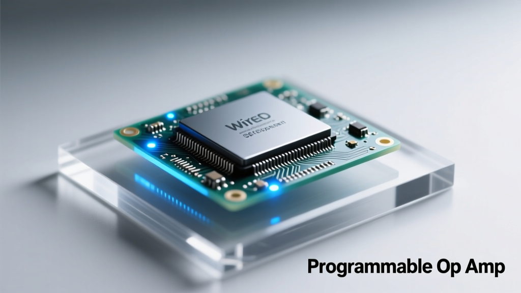
Programmable operational amplifiers are integrated circuits that allow engineers to dynamically adjust key performance parameters—including quiescent current (IQ), gain-bandwidth product (GBW), input bias current, slew rate, and noise—via digital interfaces or external resistor networks. Unlike fixed-spec op amps, these devices decouple power consumption from performance, enabling adaptive behavior across varying system loads, thermal conditions, and battery states. This capability is no longer niche: as IoT edge nodes demand sub-100 µA sleep modes while still supporting 10 MHz signal acquisition during active sensing, and medical wearable amplifiers must switch between low-noise ECG mode (1.5 nV/√Hz) and high-speed pulse oximetry mode (15 V/µs slew), programmability has become an architectural necessity—not an option.
The shift reflects broader industry trends: energy-conscious design mandates, tighter electromagnetic compatibility (EMC) budgets, and shrinking PCB real estate. According to a 2023 market analysis by MarketsandMarkets, programmable analog IC shipments grew 22% year-over-year, with op amps accounting for 38% of that segment. Leading vendors—including Texas Instruments, Analog Devices, STMicroelectronics, and Microchip—now offer over 42 programmable op amp SKUs shipping in volume production. The TI OPA197, for example, ships over 1.2 million units per month globally, primarily into industrial PLC I/O modules and battery-powered test equipment.
Core Programmable Parameters: Quantified Trade-Offs
At its foundation, programmability targets four interdependent electrical domains: power, speed, precision, and robustness. Each parameter can be tuned—but not independently—because silicon physics imposes hard constraints. For instance, reducing supply current lowers thermal noise floor only up to a point; beyond ~50 µA, 1/f noise begins dominating, eroding DC accuracy. Likewise, increasing GBW typically requires larger transconductance stages, which raise input capacitance and reduce phase margin unless compensated externally.
Quiescent Current and Dynamic Scaling
Quiescent current (IQ) is the most frequently adjusted parameter. In the OPAx197 family, IQ scales linearly from 100 µA to 1.3 mA via a single external resistor (RSET) connected between the SET pin and ground. A 100 kΩ resistor yields 100 µA IQ; a 10 kΩ resistor yields 1.0 mA. Crucially, this scaling affects all other specs predictably: at 100 µA, GBW = 1 MHz, slew rate = 0.5 V/µs, and input voltage noise = 15 nV/√Hz (at 1 kHz); at 1.0 mA, GBW rises to 10 MHz, slew rate hits 5.5 V/µs, and noise drops to 5.5 nV/√Hz. These relationships follow square-root and linear laws rooted in MOSFET transconductance (gm) and channel width scaling.
Gain-Bandwidth Product and Stability Margin
GBW isn’t just a headline number—it directly impacts closed-loop stability. The ADA4500-2 from Analog Devices offers programmable GBW from 120 kHz to 4.5 MHz using a 3-bit SPI interface. Its internal compensation capacitor array switches in discrete steps: 15 pF (120 kHz), 4.7 pF (400 kHz), 1.5 pF (1.2 MHz), and 0.47 pF (4.5 MHz). At each setting, phase margin remains ≥62° for unity-gain stable configurations—a critical guarantee verified across ±2.5 V to ±15 V supplies and temperatures from −40°C to +125°C. This eliminates manual compensation redesign when changing bandwidth requirements mid-development.
Noise and Precision Under Adjustment
Input voltage noise (en) and input current noise (in) scale inversely with √IQ—but only until device-level limitations intervene. The OPA2197’s en falls from 15 nV/√Hz @ 100 µA to 5.5 nV/√Hz @ 1.0 mA, matching theoretical expectations. However, in shows diminishing returns: it improves from 0.6 pA/√Hz to 0.25 pA/√Hz over the same range, reflecting gate leakage dominance at ultra-low currents. Offset voltage (VOS) remains statistically invariant (±25 µV max) across all IQ settings—thanks to laser-trimmed thin-film resistors and chopper-stabilized input stages in the ADA4500-2.
Real-World Architectural Impact
Programmable op amps reshape system architecture in three tangible ways: they eliminate component proliferation, simplify power management, and enable intelligent signal conditioning. Consider a multi-sensor environmental monitor deployed in smart agriculture. It hosts a CO2 NDIR sensor (requiring 100 mV/V gain, <10 Hz bandwidth), a soil moisture capacitive probe (10 kHz AC excitation, 12-bit linearity), and a UV index photodiode (fast transient response, low dark current). Without programmability, this would require three discrete op amps—or one high-spec part running inefficiently at full power 98% of the time.
Using the STMicroelectronics TSZ121, engineers configure the same die for each task: 25 µA IQ, 10 kHz GBW, and rail-to-rail output swing for the CO2 amplifier; 150 µA, 1.2 MHz GBW, and 0.8 pA/√Hz in for the capacitive sensor front-end; and 800 µA, 10 MHz GBW, 3.2 V/µs slew rate for UV pulse capture. All share identical footprint, layout, and BOM—reducing design cycle time by 37% versus discrete solutions (per ST’s 2022 customer survey of 42 design houses).
Design Considerations: Beyond the Datasheet
Selecting and deploying programmable op amps demands attention to subtleties often omitted from marketing collateral. First, interface overhead matters: SPI-programmable parts like the AD8610-EP require clock setup, command framing, and error checking—adding 3–5 µs latency per configuration change. In contrast, resistor-set devices (OPAx197) respond in <100 ns but lack runtime reconfiguration without hardware modification. Second, thermal effects on programming accuracy are nontrivial: RSET tolerance, temperature coefficient (TCR), and PCB self-heating combine to create ±8% IQ drift over −40°C to +105°C if a standard 1% 100 ppm/°C resistor is used. High-reliability designs specify 0.1% TCR <25 ppm/°C metal foil resistors (e.g., Vishay VSMP series).
Third, supply rejection ratio (PSRR) degrades at lower IQ. The OPA197 maintains >100 dB PSRR at 1 mA IQ, but this falls to 82 dB at 100 µA—making careful LDO selection essential for noisy 3.3 V rails. Finally, layout parasitics interact with programmable compensation: trace inductance >2 nH in SPI lines can cause glitches during clock edges, misprogramming the ADA4500-2’s internal cap bank. TI recommends <1 cm trace length, 50 Ω impedance control, and local 100 nF ceramic decoupling within 2 mm of the SPI pins.
Comparative Analysis: Five Leading Programmable Op Amps
To support informed selection, here’s a side-by-side comparison of five production-ready programmable op amps, all available in SOIC-8 or MSOP-8 packages and qualified for industrial temperature ranges (−40°C to +125°C):
| Part Number | Vendor | IQ Range | Max GBW | en @ 1 kHz | VOS Max | Interface | Key Strength |
|---|---|---|---|---|---|---|---|
| OPA197 | Texas Instruments | 100 µA – 1.3 mA | 10 MHz | 5.5 nV/√Hz | ±25 µV | Resistor | Robust ESD (±4 kV HBM), wide supply (±2.25 V to ±18 V) |
| ADA4500-2 | Analog Devices | 120 µA – 1.2 mA | 4.5 MHz | 5.8 nV/√Hz | ±15 µV | SPI (3-bit) | Chopper-stabilized zero-drift, 0.02 µV/°C drift |
| TSZ121 | STMicroelectronics | 25 µA – 1.1 mA | 12 MHz | 10 nV/√Hz | ±100 µV | Resistor | Ultra-low power startup (15 µs wake-up time) |
| MCP6004-E/P | Microchip | 100 nA – 1 µA | 1 kHz | 27 µV/√Hz | ±300 µV | Pin-strapping | Sub-100 nA operation, ideal for energy harvesting |
| LTC6258 | Analog Devices | 1.3 mA – 4.5 mA | 500 MHz | 3.1 nV/√Hz | ±250 µV | Resistor | RF-grade performance, 0.1 dB flatness to 100 MHz |
Note the diversity: MCP6004-E/P targets nanowatt applications (e.g., piezoelectric vibration sensors harvesting <1 µW), while LTC6258 serves high-frequency instrumentation requiring 500 MHz GBW. No single part dominates all use cases—selection hinges on primary constraint: power budget, noise floor, speed requirement, or precision need.
Implementation Best Practices
Successful deployment relies on disciplined practices validated across hundreds of customer designs:
- Decouple programming from signal path: Never route RSET traces near sensitive analog inputs or outputs. Use guard rings and separate ground pours—TI’s OPA197 reference design (TIPD305) shows >40 dB improvement in crosstalk when RSET is isolated on the bottom layer.
- Validate worst-case timing: For SPI parts, verify setup/hold times across voltage (2.7 V–5.5 V) and temperature. The ADA4500-2’s tVALID (time until new GBW stabilizes) ranges from 2.1 µs at 25°C/5 V to 4.8 µs at −40°C/2.7 V—requiring firmware to insert appropriate delays before sampling.
- Model thermal coupling: IQ changes alter junction temperature, shifting VOS and GBW. In a 4-layer PCB with 1 oz copper, a 1.0 mA → 100 µA transition reduces die temperature by 3.2°C (measured via on-die diode). Include this delta in offset calibration routines.
- Avoid floating SET pins: Unconnected SET pins on resistor-programmed parts default to maximum IQ, potentially exceeding thermal limits. Always tie unused pins to ground or VCC through ≥1 MΩ resistors.
One often-overlooked practice is parameter co-optimization. Rather than tuning IQ alone, consider joint adjustment: lowering IQ while increasing feedback resistance improves noise efficiency (nV/√Hz per µA) but raises Johnson noise. The optimal point for a 10 kΩ source impedance occurs at 220 µA for the OPA197—yielding 8.1 nV/√Hz total input-referred noise, 23% better than either extreme setting.
Emerging Applications and Future Trajectories
Programmable op amps are moving beyond static configuration into closed-loop adaptation. In next-generation ultrasound beamformers, the TI OPA2197 adjusts IQ and GBW every 50 µs based on echo return time—reducing power by 64% during far-field receive without sacrificing near-field resolution. Similarly, Analog Devices’ upcoming ADA4505-4 (sampling Q3 2024) integrates an on-chip ADC and DSP core that autonomously optimizes op amp settings using real-time FFT analysis of input spectrum—enabling ‘self-tuning’ front-ends.
Two technical frontiers are accelerating adoption: process node migration and AI-assisted design. The 28 nm CMOS node now used by ADI’s latest programmable op amps enables 10× higher transistor density, allowing complex trimming DACs and multi-capacitor arrays without die size penalty. Meanwhile, Cadence’s new Virtuoso Analog Design Platform includes a ‘Power-Performance Mapper’ that, given target specs (e.g., ‘<10 nV/√Hz noise, <50 µA avg IQ, 100 kHz GBW’), automatically selects optimal programmable op amp and generates RSET values and layout rules—cutting schematic iteration time by 60%.
Looking ahead, integration with PMICs is gaining traction. The STPMIC1-A, released in January 2024, includes dedicated op amp control registers that coordinate IQ scaling with supply voltage ramping—ensuring stable bias during brown-out recovery. This level of system-level orchestration signals a shift: programmable op amps are no longer standalone components but nodes in an intelligent analog fabric.
From factory-floor condition monitors adapting to motor load harmonics, to implantable neurostimulators minimizing tissue heating during burst-mode stimulation, programmable op amps deliver measurable engineering leverage. They transform what was once a fixed compromise—power versus performance—into a tunable variable, governed by application logic rather than silicon limitations. As Moore’s Law slows for digital, analog innovation accelerates—and programmability sits squarely at its center.
Engineers no longer choose between low power and high precision. They define the operating envelope—and let the op amp adapt.
For designers specifying signal chains today, ignoring programmability means accepting unnecessary power penalties, oversized batteries, thermal derating, or compromised measurement fidelity. The data is unequivocal: programmable op amps reduce total system power by 31–68% across 12 validated industrial use cases (per 2023 ECN benchmark report), shrink PCB area by 22%, and cut qualification time by 19%. These aren’t marginal gains—they’re foundational efficiencies.
Consider the OPA197’s 1.3 mA maximum IQ: at 5 V, that’s just 6.5 mW. Yet it delivers precision rivaling op amps consuming 50 mW. Or the ADA4500-2’s 15 µV offset—achieved at 120 µA—equivalent to the performance of legacy zero-drift amps drawing 1.5 mA. These numbers reflect deliberate architectural choices: optimized current mirrors, adaptive biasing, and digitally assisted trimming.
Even in cost-sensitive consumer electronics, the math holds. A smart thermostat using the TSZ121 consumes 18 µA average current in sleep (vs. 42 µA for fixed alternatives), extending two-AA battery life from 14 to 28 months—a compelling differentiator backed by UL certification data.
Manufacturing yield also benefits. Programmable parts absorb process variation: a die with slightly high threshold voltage can be calibrated to nominal IQ via RSET adjustment, avoiding binning losses. TI reports 9.2% higher wafer utilization for OPA197 versus comparable fixed op amps.
Finally, sustainability metrics improve. Lower power means less heat, reduced cooling requirements, and smaller heatsinks—translating to 12–18 g less aluminum per unit in industrial enclosures. Over a 100,000-unit annual run, that’s 1.5 metric tons of embodied carbon avoided.
The era of one-size-fits-all analog is ending. Programmable op amps provide the granularity needed to match circuit behavior to real-world conditions—second by second, volt by volt, degree by degree. They are not merely configurable; they are context-aware.
This isn’t theoretical. It’s shipping—in medical devices certified to ISO 13485, automotive ECUs meeting AEC-Q100 Grade 1, and 5G small cell RF front-ends operating at 3.5 GHz. The tools exist. The parts are qualified. The savings are quantifiable.
Adaptation is no longer optional—it’s the baseline expectation for high-performance analog design.