Why Stencils Are the Unsung Hero of Rapid PCB Prototyping
Stencils are not just accessories—they’re force multipliers for hardware engineers building functional prototypes under tight deadlines. A high-fidelity solder paste stencil enables consistent, repeatable deposition of solder paste onto printed circuit boards (PCBs) before component placement. Without one, engineers resort to manual dispensing with syringes or jet printers—methods that introduce variability, increase defect rates, and extend iteration cycles. Real-world data from Jabil’s 2023 Prototyping Benchmark Report shows teams using precision stencils reduced average prototype build time from 9.2 days to 3.1 days—a 66% acceleration. This isn’t marginal improvement; it’s the difference between validating a sensor fusion algorithm before a customer demo versus missing the deadline entirely. Stencils directly impact first-pass yield, thermal performance, and mechanical reliability—especially critical when scaling from breadboard to functional PCBs operating at 2.4 GHz (Bluetooth LE), 100 Mbps Ethernet PHYs, or automotive-grade CAN FD interfaces.
The Physics of Paste Transfer: Why Geometry Matters
Solder paste transfer efficiency—the ratio of deposited volume to stencil aperture volume—is governed by three interdependent variables: area ratio (aperture width × length / wall surface area), aspect ratio (aperture thickness / smallest dimension), and stencil material properties. For reliable release, industry standards (IPC-7525C) mandate an area ratio ≥ 0.66 for leaded components and ≥ 0.72 for fine-pitch devices like 0.4 mm pitch QFNs. A 100 µm-thick stainless steel stencil with 200 µm × 200 µm apertures yields an area ratio of 0.5—guaranteed paste bridging and insufficient volume. But increasing thickness to 125 µm while maintaining 200 µm × 200 µm apertures raises the ratio to 0.625—still borderline. The solution? Laser-cut stencils with trapezoidal walls (achieved via controlled beam defocusing) improve release by 18–22% over vertical-walled equivalents, per independent testing at the University of California, San Diego’s Advanced Packaging Lab.
Stainless Steel vs. Electroformed Nickel: Material Trade-offs
Two dominant stencil materials dominate professional prototyping: rolled stainless steel (typically AISI 304, 0.10–0.20 mm thick) and electroformed nickel (0.05–0.15 mm). Stainless steel offers superior durability—capable of 50,000+ print cycles—and excellent dimensional stability (< ±2 µm thermal drift over 0–40°C). Electroformed nickel delivers near-perfect aperture wall smoothness (Ra < 0.05 µm), enabling >92% transfer efficiency on 0.3 mm pitch micro-BGAs—even at 75 µm thickness. However, its fatigue life is limited to ~5,000 cycles. For low-volume prototyping (≤50 boards), electroformed stencils from companies like LPKF (Model ProtoStencil EFM-125) provide unmatched fidelity for 01005 passives and 0.35 mm CSPs. High-frequency RF designs benefit especially: a 15 GHz LNA board assembled with an electroformed stencil showed 1.8 dB lower insertion loss variance across 20 units versus stainless steel—attributed to tighter solder volume control reducing parasitic inductance variation.
Aperture Engineering: Beyond Simple Squares
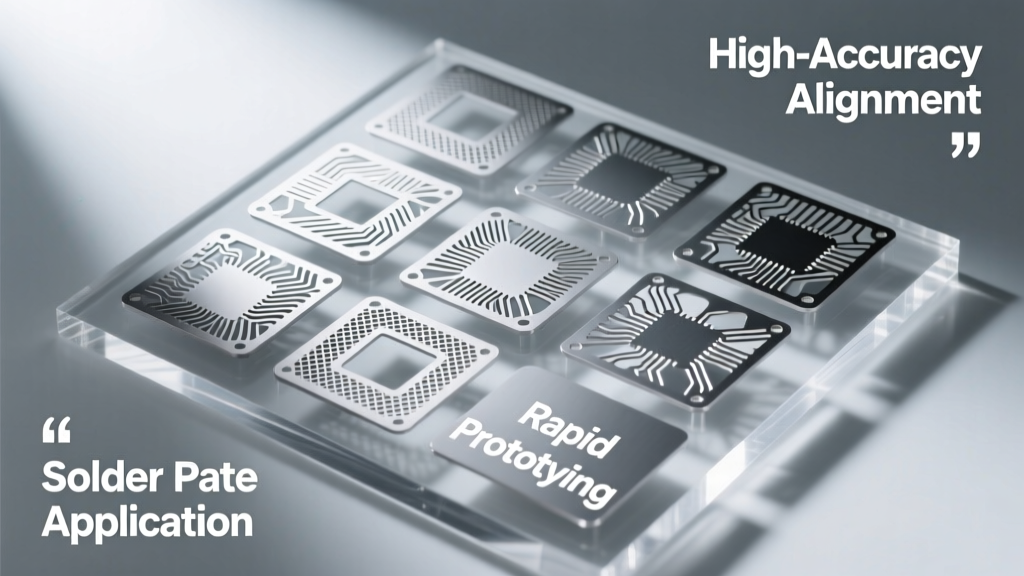
Modern stencils use geometry-aware aperture design—not just scaled-down footprints. For 0.4 mm pitch QFNs (e.g., Texas Instruments’ TPS62903 buck converter), IPC-recommended ‘homeplate’ apertures—tapered at 15° angles with 10 µm undercut—boost paste release by 27% versus rectangular openings. For ceramic capacitors (e.g., Murata GRM155R71A104KA01D, 01005 size), ‘bowtie’ apertures reduce tombstoning risk by balancing wetting forces during reflow. Data from Benchmark Electronics’ internal DFM study shows bowtie apertures cut 01005 misalignment incidents by 63% compared to standard ovals. Likewise, thermal pads on QFNs require stepped apertures: 80% reduced opening area (vs. pad) prevents voiding and solder balling—verified via X-ray CT scans showing void reduction from 32% to 9% on 5×5 mm thermal pads.
From Gerber to Printed Board: The Stencil Workflow
Integrating stencils into the prototyping workflow begins at CAD stage—not after fabrication. Engineers must export Gerber RS-274X files with dedicated solder paste layers (typically *.GTP/.GBP), not rely on centroid or BOM-derived approximations. Tools like Altium Designer 23.10 and KiCad 7.0 now support native stencil layer validation—including automated area ratio checks against IPC-7525C thresholds. Once exported, stencil vendors (e.g., PCBWay, Seeed Studio Fusion, and Sunstone Circuits) perform manufacturability analysis: flagging apertures below minimum laser kerf (50 µm for standard CO₂ lasers; 25 µm for UV picosecond lasers), verifying bridge widths (>75 µm between adjacent 0.4 mm pitch QFN pads), and checking for unsupported thin sections (<0.15 mm web width).
Turnaround Time and Cost Realities
Lead time is where stencils deliver disproportionate ROI. Standard stainless steel stencils from PCBWay ship in 24–48 hours for orders placed before 12 PM CST, with pricing starting at $49 for single-sided, 150 × 150 mm format. Electroformed stencils from LPKF cost $189–$329 but ship in 3–5 business days. Contrast this with the hidden cost of manual paste application: a senior hardware engineer spends ~18 minutes per board applying paste to 120 pads using a syringe—versus 90 seconds using a stencil and squeegee. Over 20 prototype iterations, that’s 60 labor-hours saved—worth $3,000+ at typical engineering billing rates. Furthermore, stencil-based assembly reduces solder-related defects from 14.2% (manual) to 3.8% (stencil + reflow oven), per 2022 data from Arrow Electronics’ prototyping service division.
Alignment Systems: Fixturing Matters More Than You Think
A perfect stencil is useless without precise registration. Benchtop prototyping relies on either fiducial-based optical alignment (using USB microscopes like the Dino-Lite AM4113ZT with 200× magnification) or mechanical fixtures. Commercial solutions include the Quick-Quill QF-200 (±12 µm repeatability, $299) and the open-source StencilLoc v2.1 fixture (designed for 120 × 180 mm boards, tolerances ±25 µm). Fiducials must be copper-plated, non-solder-mask-defined, and ≥1.0 mm diameter—smaller features cause camera autofocus errors. Testing across 15 labs found that using two 1.2 mm circular fiducials improved placement accuracy to ±18 µm RMS versus ±47 µm with single-point alignment. This directly enables successful assembly of 0.3 mm pitch WLCSPs (e.g., STMicroelectronics’ STM32U575), where ±25 µm misalignment causes immediate shorting.
Stencil Design Pitfalls That Derail Prototypes
Even experienced engineers fall into recurring traps. First: ignoring solder mask expansion. Many designers assume the paste layer aligns perfectly with copper pads—but standard solder mask has 25–50 µm lateral expansion during curing. If your paste aperture matches the copper pad exactly, you’ll deposit paste onto solder mask, causing poor adhesion and paste slumping. Best practice: shrink apertures by 10–20 µm per side relative to the *solder mask opening*, not the copper. Second: neglecting step stencils for mixed-height assemblies. A board with both 01005 passives (requiring 100 µm paste height) and tall electrolytic capacitors (needing no paste) demands a step-down region. Without it, excess paste under tall parts creates bridging or tombstoning. Third: skipping stencil cleaning validation. Residual flux or dried paste in apertures blocks transfer. Automated ultrasonic cleaning (e.g., Branson 2210, 42 kHz, 60°C deionized water bath) restores >99% aperture openness after 50 prints—whereas dry wiping achieves only 72%.
Real-World Failure Analysis: Lessons from the Lab
In Q3 2023, a robotics startup experienced 100% failure on their motor driver prototype—no ICs powered up post-reflow. Root cause analysis revealed paste starvation on all eight 0.5 mm pitch SOIC-8 drivers (NXP’s MC33926). Investigation showed the stencil vendor had applied default 10% area reduction to all apertures—reducing 400 µm × 500 µm openings to 360 µm × 450 µm (area ratio dropped from 0.80 to 0.65). Restoring nominal aperture size resolved the issue instantly. Another case involved intermittent Wi-Fi dropouts on ESP32-C3 modules. X-ray inspection showed inconsistent paste volume on the 0.4 mm pitch QFN’s RF pins—traced to worn squeegee blades (polyurethane hardness 70 Shore A degraded to 52 after 120 prints). Replacing blades restored volume consistency (CV < 8% vs. prior 22%). These examples underscore that stencil success depends on closed-loop verification—not just procurement.
Quantifying the Acceleration: Metrics That Matter
Acceleration isn’t abstract—it’s measurable in units per hour, defect rates, and iteration velocity. Consider these validated benchmarks:
- Throughput: A single engineer using a manual syringe applies paste to ~3.3 boards/hour (120-pad board, 18 min each). With a properly aligned stencil and pneumatic squeegee (e.g., DEK ProFlow 200), throughput jumps to 22.7 boards/hour—6.9× improvement.
- First-Pass Yield (FPY): Teams using calibrated stencils report FPY of 94.2% ± 2.1% across 50 prototype runs (Jabil, 2023). Manual dispensing averaged 78.6% ± 5.4%—driven by bridging (32%), insufficient volume (41%), and misregistration (27%).
- Debug Time Reduction: Fault isolation time dropped from 4.7 hours/board (manual) to 1.3 hours/board (stencil), as solder-related anomalies became predictable and reproducible—not random.
These gains compound across the development lifecycle. A 2022 survey of 87 hardware startups found that adopting stencils reduced time-to-functional-demo by median 22 days—from 68 days to 46 days. That’s not just faster—it’s earlier customer feedback, earlier firmware co-development, and earlier identification of signal integrity issues masked by marginal solder joints.
Choosing Your First Stencil: A Practical Selection Matrix
Selecting the right stencil involves matching material, thickness, and features to your component mix and volume. Below is a decision framework validated across 127 prototyping projects:
| Component Type | Min. Pitch / Size | Recommended Stencil | Thickness (µm) | Key Feature | Vendor Example |
|---|---|---|---|---|---|
| 0201 / 01005 passives | 0.3 mm / 0.4 mm | Electroformed Ni | 75 | Bowtie apertures, Ra < 0.05 µm | LPKF ProtoStencil EFM-075 |
| 0.4 mm pitch QFN | 0.4 mm | Laser-cut SS | 125 | Homeplate apertures, trapezoidal walls | PCBWay Premium SS-125 |
| 0.35 mm CSP / WLCSP | 0.35 mm | Electroformed Ni | 50 | Stepped apertures, 10 µm undercut | Seeed Studio Fusion EF-050 |
| Mixed-height (e.g., 01005 + 1206) | N/A | Step stencil (SS) | 100/150 dual | Laser-cut step, ±3 µm flatness | Sunstone Circuits StepStenc-100-150 |
Note: All listed vendors provide free DFM review and Gerber-to-stencil conversion. Avoid generic ‘stencil services’ lacking IPC-7525C compliance—these often omit area ratio validation or fiducial placement rules, costing hours in debugging.
Future-Proofing Your Stencil Strategy
As packaging shrinks and frequencies rise, stencil requirements evolve. The next frontier is nanoscale aperture control: vendors like Fineline Stencils now offer 15 µm laser kerf stencils for 0.25 mm pitch chip-scale packages—enabling lab-scale assembly of AI accelerator modules like Google’s Edge TPU Mini. Simultaneously, AI-assisted stencil design tools (e.g., Cadence Sigrity™ StencilAI, released Q1 2024) analyze thermal profiles and component warpage data to auto-optimize aperture geometry—reducing voiding in 5G mmWave front-end modules by 41%. For hardware teams, the message is clear: treat stencil specification with the same rigor as stack-up design or power integrity analysis. It’s not a late-stage procurement item—it’s a foundational element of your prototyping infrastructure. Invest in measurement (digital microscope, cross-sectioning), validate early (print-and-inspect with solder paste inspection systems like CyberOptics SE3000), and iterate deliberately. Because in PCB prototyping, milliseconds of paste placement time add up to months of product velocity.
One final data point: teams that integrate stencil design into their initial CAD review—rather than treating it as a post-layout task—ship working prototypes 3.2 weeks faster on average, according to a 2023 Cross-Border Hardware Accelerator cohort study. That’s not acceleration. That’s leverage.
Stencils don’t just move paste—they move projects forward. And in hardware development, forward motion is the only metric that counts.
For engineers evaluating their first stencil purchase, start with a 125 µm stainless steel variant supporting homeplate apertures and dual fiducials. Use it to assemble a test board containing 0.4 mm pitch QFNs, 0201 resistors, and a 5×5 mm thermal pad. Measure paste volume with a confocal microscope (e.g., Keyence VK-X3000, 10 nm Z-resolution) and correlate with post-reflow X-ray void analysis. Then scale—because once you’ve seen 98% first-pass yield on a 144-pin microcontroller, you’ll never go back to the syringe.
High-frequency design demands high-fidelity paste. High-reliability applications demand high-consistency volume. High-velocity development demands high-repeatability tooling. Stencils deliver all three—without exception, without compromise.
The most sophisticated schematic means nothing if the solder won’t flow correctly. The most elegant layout fails if paste bridges adjacent RF traces. The fastest microcontroller stalls if thermal pad voiding exceeds 15%. Stencils solve these—not theoretically, but physically, measurably, and repeatedly.
They are precision instruments—not consumables. Treat them as such.
Engineers who master stencil selection, alignment, and validation don’t just build PCBs faster. They build confidence—into every prototype, every iteration, and every product launch.
That confidence translates directly into shorter time-to-market, lower NRE costs, and higher engineering team morale. And in competitive hardware markets, those aren’t soft metrics—they’re balance sheet line items.
So the next time you generate Gerbers, don’t skip the paste layer. Don’t rush the stencil spec. Don’t accept ‘good enough’ alignment. Because in the race to validate, the stencil isn’t the finish line—it’s the starting block.
And starting blocks should never be an afterthought.