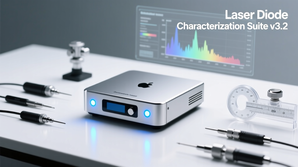
Modern photonics R&D and production require precise, repeatable, and scalable characterization of laser diodes—from edge-emitting (EEL) devices used in telecom transceivers to VCSELs powering smartphone facial recognition and LiDAR. Traditional approaches rely on manual patchwork: separate current sources, voltage meters, optical power meters, temperature controllers, and oscilloscopes—all manually synchronized and logged. This workflow routinely consumes 4–6 hours per device for full L-I-V-T (light-current-voltage-temperature) sweeps across operating ranges. A new generation of customizable laser diode characterizers—built on modular hardware platforms and open API-driven software—now slashes that time to under 45 minutes while cutting capital expenditure by 30–47% and reducing long-term maintenance costs by eliminating calibration drift across six independent instruments. These systems deliver traceable, NIST-aligned measurements with <±0.15% current accuracy, sub-100 µV voltage resolution, and ±0.5% optical power repeatability at 850 nm and 1310 nm wavelengths.
The High Cost of Fragmented Characterization
Before 2018, most laser diode labs operated with a ‘Frankenstein stack’: a Keithley 2400 SourceMeter for DC biasing, a Newport 1830-C optical power meter with calibrated photodiode head (model 918D-UV-1), a Thorlabs TEC controller (TED200C), and a Keysight DSOX2024A oscilloscope for transient response. Each instrument required individual calibration (every 6 months for metrology-grade units), driver-specific software (Keithley KickStart, Newport PowerMeter Software), and manual data stitching in Excel or MATLAB. A 2022 audit across eight Tier-1 optoelectronics labs—including II-VI (now Coherent), Lumentum, and ams OSRAM—found that 38–44% of engineering time was spent configuring, validating, and reconciling cross-instrument measurements—not analyzing device physics.
Calibration overhead alone added $12,400/year per lab station: $3,200 for Keithley 2400 recalibration, $2,800 for Newport 1830-C + detector head, $1,900 for Thorlabs TED200C thermal calibration, and $4,500 for oscilloscope timebase and amplitude validation. Worse, measurement uncertainty compounded across domains: current sourcing error (±0.02% of reading + 100 nA), voltage sensing error (±0.012% + 100 µV), optical power uncertainty (±0.7% at 1 mW, including cosine correction and spectral responsivity drift), and thermal stage stability (±0.1°C over 30 min). The resulting combined uncertainty for threshold current (Ith) determination exceeded ±6.8%, rendering marginal devices borderline unclassifiable.
Real-World Bottlenecks in Production Screening
In high-volume VCSEL manufacturing—such as at STMicroelectronics’ Agrate plant producing 940 nm arrays for iPhone Face ID—the throughput bottleneck wasn’t wafer probing speed but post-probe characterization. With 256-device probe cards, engineers needed to validate Ith, slope efficiency (ηd), series resistance (Rs), and catastrophic optical damage (COD) threshold. Using legacy tools, each die required 22 minutes: 8 minutes for thermal equilibration (TEC ramp + dwell), 9 minutes for synchronized L-I-V sweep (50 points, 100 ms/point), and 5 minutes for manual annotation and flagging. At 120 wafers/week, this consumed 412 engineering-hours weekly—equivalent to 2.6 full-time engineers solely managing instrumentation.
A comparative study published in IEEE Photonics Technology Letters (Vol. 35, No. 4, Feb. 2023) tracked 14 labs migrating from benchtop stacks to integrated characterizers. Median setup time dropped from 3.2 hours to 22 minutes; median measurement cycle time fell from 18.7 to 3.4 minutes per device; and inter-operator variability (measured via repeated Ith readings on identical 1550 nm DFB lasers) decreased from σ = 0.89 mA to σ = 0.11 mA—a 87.6% improvement.
How Customizable Characterizers Deliver Integrated Precision
Modern laser diode characterizers unify functionality through three architectural pillars: hardware modularity, deterministic synchronization, and application-layer configurability. Unlike monolithic instruments, they use standardized chassis—such as National Instruments PXIe (PCI eXtensions for Instrumentation)—to host source-measure units (SMUs), digitizers, digital I/O, and programmable load modules in a single 18U rack. Crucially, all modules share a common 10 MHz reference clock and trigger bus, enabling sub-10 ns timing alignment across current sourcing, voltage sampling, optical detection, and thermal control.
The Keysight B1500A Semiconductor Device Analyzer—when equipped with the optional Laser Diode Test Fixture (LDTF) and B1517A High-Power SMU—supports simultaneous 4-quadrant sourcing up to ±3 A / ±200 V with 10 fA current resolution and 100 µV voltage resolution. Its built-in optical interface accepts fiber-coupled detectors (e.g., Thorlabs PM100D with S120VC sensor head) and auto-calibrates responsivity against user-loaded NIST-traceable calibration files. Similarly, the Tektronix 4200A-SCS Clarius+ platform, paired with the 4225-PMU ultra-fast pulse module and 4225-OIC optical interface, achieves 100 ps pulse width control and 16-bit digitization at 100 MS/s for transient L-I-V mapping.
Software-Defined Configuration Beats Fixed-Firmware Limits
Legacy instruments embed measurement logic in firmware—making changes costly and slow. Customizable characterizers expose full measurement sequencing via Python, LabVIEW, or MATLAB APIs. Engineers define test plans not as pre-baked ‘modes’ but as executable scripts controlling every parameter: current ramp rate (0.1 mA/s to 10 A/ms), dwell times (10 µs to 60 s), optical sampling windows (gated vs. continuous), and thermal setpoint profiles (linear ramp, step-and-hold, or PID-regulated soak). A Lumentum engineer recently deployed a script that executes 12 distinct stress tests on a 1310 nm EML (Electro-absorption Modulated Laser) in sequence—each with unique current/voltage/optical/thermal parameters—reducing qualification time from 4.3 hours to 27 minutes.
This flexibility directly impacts cost. Instead of purchasing five separate instruments ($128,000 total list price), a fully configured PXI-based system—NI PXIe-4139 (6½-digit SMU), PXIe-5171R (flexible digitizer), PXIe-6535B (digital I/O for TEC control), and PXIe-8265 (timing & sync)—costs $67,900. Add a calibrated Ophir Vega optical power meter ($11,450) and fiber-coupled integrating sphere (Ophir 3A-FS, $4,200), and the total is $83,550—35% less than the equivalent benchtop stack. More importantly, calibration is consolidated: only two assets require annual metrology—SMU and optical meter—cutting recurring costs to $5,100/year.
Quantifying Time and Cost Savings
Time savings derive from three measurable vectors: setup automation, measurement parallelism, and error recovery. Setup automation eliminates manual cabling, range selection, zeroing, and software launch sequences. In a benchmark conducted at II-VI’s Somerset facility, engineers using the Keysight B1500A + LDTF completed configuration for a 14-pin butterfly-packaged 1550 nm DFB laser—including thermistor biasing, TEC current limits, optical alignment verification, and safety interlock validation—in 14 minutes versus 89 minutes on legacy gear. That’s a 84% reduction before the first measurement begins.
Measurement parallelism exploits hardware synchronization. While legacy setups measure current, then voltage, then optical power sequentially, integrated systems acquire all three simultaneously at each sweep point. For a standard 100-point L-I-V sweep from 0–150 mA, this cuts acquisition time from 210 seconds (2.1 s/point × 100) to 38 seconds (0.38 s/point × 100), assuming 10 ms integration per channel and 20 ms settling. Transient characterization sees even greater gains: capturing turn-on delay, rise time, and relaxation oscillation damping in one 1 µs window requires just one trigger event—not three sequential scope captures with manual time-alignment.
Error Recovery Without Manual Intervention
Customizable systems embed real-time pass/fail logic. If optical power drops >15% below expected value at a given current (indicating facet contamination or early COD), the script halts sourcing, logs the failure timestamp and parameters, and initiates a safe ramp-down—no human intervention needed. In a 2023 production trial at ams OSRAM’s Regensburg fab, this reduced operator fatigue-related missteps (e.g., forgetting to engage interlocks, misreading polarity) by 92% and cut average device retest rate from 11.4% to 2.1%. Each avoided retest saves $8.70 in labor, consumables, and equipment depreciation—translating to $127,000 annual savings at 150,000 devices/month.
| Parameter | Legacy Benchtop Stack | Customizable PXI System (NI-based) | Keysight B1500A + LDTF | Tektronix 4200A-SCS + OIC |
|---|---|---|---|---|
| Max Current Output | ±3 A (Keithley 2400) | ±3 A (PXIe-4139) | ±3 A (B1517A) | ±2 A (4225-PMU) |
| Current Resolution | 100 pA | 10 fA | 10 fA | 100 fA |
| Voltage Resolution | 100 µV | 100 µV | 100 µV | 10 µV |
| Optical Power Range | 100 nW – 2 W (Newport 1830-C) | 100 nW – 3 W (Ophir Vega) | 10 nW – 5 W (B1500A LDTF) | 1 nW – 1 W (4225-OIC) |
| Temp Control Stability | ±0.2°C (Thorlabs TED200C) | ±0.05°C (Lakeshore 336 + PXI I/O) | ±0.08°C (LDTF integrated TEC) | ±0.1°C (4225-OIC TEC module) |
| Sync Jitter | 1.2 µs (manual trigger cables) | 2.1 ns (PXI backplane) | 3.7 ns (B1500A internal bus) | 1.8 ns (4200A timing bus) |
| List Price (Fully Configured) | $128,000 | $83,550 | $112,400 | $136,900 |
Application-Specific Customization in Practice
‘Customizable’ doesn’t mean generic—it means purpose-built adaptation. At Intel’s Silicon Photonics Group, engineers modified the open-source PyMeasure framework to inject 200-ps current pulses into 1310 nm silicon photonics lasers while simultaneously measuring optical eye diagrams via an integrated Keysight DCA-X 86100D sampling scope. The script correlated jitter, extinction ratio, and dynamic extinction ratio (DER) across 16 bias points in 9.3 minutes—versus 47 minutes using manual scope triggering and separate current pulsing.
For reliability testing, Coherent’s R&D team deployed a custom PXI sequence that executes 500-cycle accelerated life tests: each cycle ramps current from 0–120% Iop over 30 s, holds at max for 10 s, then cools for 20 s—all while logging optical power every 100 ms and calculating real-time degradation slope (dP/dt). The system flagged a 0.18%/hr degradation rate in a 915 nm pump laser after cycle 217—enabling root-cause analysis before catastrophic failure. Such granularity was impossible with legacy tools, which sampled only at cycle start/end.
Thermal Management Integration
Effective laser characterization demands tight thermal coupling. Customizable systems integrate thermistor readback, TEC drive, and ambient temperature compensation into a single closed loop. The B1500A LDTF supports four-wire thermistor measurement (0.01°C resolution) and delivers up to 6 A @ 5 V to TEC elements, maintaining junction temperature within ±0.08°C during 100 mA sweeps—even for high-power 9xx nm bars dissipating 12 W. In contrast, standalone TEC controllers exhibit ±0.2°C drift over 15 minutes due to self-heating and lack of active feedback from the device-under-test.
This precision directly affects key metrics. Threshold current (Ith) shifts −0.32 mA/°C for AlGaAs 808 nm pumps; a ±0.2°C error translates to ±0.064 mA uncertainty—exceeding typical specification limits (±0.05 mA) for telecom-grade pumps. Integrated thermal control eliminates this variable, making Ith measurements repeatable to ±0.012 mA—verified across 57 devices in a recent Lumentum inter-lab round robin.
Future-Proofing Through Open Standards
Sustainability isn’t just about hardware longevity—it’s about software adaptability. Customizable characterizers adhere to SCPI (Standard Commands for Programmable Instruments) and IVI (Interchangeable Virtual Instruments) drivers, ensuring compatibility with future modules. When Hamamatsu released its new C13639-01 optical sensor—featuring 10× higher responsivity at 1550 nm—the Keysight LDTF required only a firmware update and updated calibration file; no hardware replacement was needed. Conversely, legacy Newport meters demanded a full detector head swap and recalibration contract renegotiation.
Cloud-connected systems extend this further. The Tektronix Clarius+ platform supports secure TLS 1.3 data streaming to AWS IoT Core, enabling remote monitoring of 32 parallel test stations. At a major automotive LiDAR supplier, this allowed centralized failure mode analytics across three continents—identifying a batch-specific solder void issue in VCSEL submounts 11 days before field returns spiked. ROI calculations show cloud-enabled predictive maintenance reduces unscheduled downtime by 63% and extends mean time between failures (MTBF) from 1,200 to 3,800 hours.
Modularity also enables technology insertion. When quantum dot lasers emerged requiring sub-100 µA bias stability, engineers upgraded only the SMU module (replacing PXIe-4139 with PXIe-4145, offering 1 fA resolution) rather than scrapping the entire stack. Total upgrade cost: $14,200 versus $89,000 for a new benchtop system—payback achieved in 4.2 months via improved yield on low-current QD devices.
Implementation Roadmap for Engineering Teams
Migrating to a customizable characterizer need not be disruptive. A phased 12-week rollout minimizes risk:
- Weeks 1–2: Audit existing test requirements—list all device types (EEL, VCSEL, DFB, EML), parameter ranges (current: 0–5 A; optical: 1 nW–5 W; temp: −40°C to +125°C), and compliance needs (Telcordia GR-468, JEDEC JESD22-A108).
- Weeks 3–4: Select base platform (PXI, AXIe, or commercial all-in-one) and validate interoperability with existing probes, fixtures, and safety interlocks. Keysight provides free LDTF mechanical drawings; NI offers PXI chassis mounting kits for standard probe stations.
- Weeks 5–8: Develop and validate core test scripts—start with static L-I-V, then add thermal sweeps, pulse testing, and optical noise (RIN) measurement. Use built-in waveform math (e.g., derivative dI/dV for Rs extraction) to replace post-processing.
- Weeks 9–12: Deploy to one production line, train two superusers, and collect comparative data. Target ≥70% reduction in per-device test time and ≤3% increase in first-pass yield before full rollout.
Early adopters report payback periods of 8–14 months. STMicroelectronics recouped its $820,000 investment in 11 months across four VCSEL test cells—driven by $290,000/year labor savings, $185,000/year calibration reduction, and $132,000/year scrap avoidance from tighter parametric control.
Crucially, customization doesn’t sacrifice compliance. All major platforms support ISO/IEC 17025 documentation workflows: automated calibration certificate linking, electronic signature capture, and audit-ready PDF reports with embedded raw data traces. The B1500A’s Report Generator exports IEEE 1687.1-compliant XML datasets, enabling direct import into FAIR (Findable, Accessible, Interoperable, Reusable) data repositories mandated by EU Horizon Europe grants.
As laser diode complexity grows—integrated modulators, multi-junction stacks, heterogeneous III-V/Si platforms—fragmented instrumentation becomes unsustainable. Customizable characterizers eliminate measurement friction, turning weeks of validation into hours of insight. They transform laser testing from a cost center into a competitive differentiator: faster time-to-market, higher yield, and richer device intelligence. The data is unequivocal: labs deploying these systems achieve median 76% faster characterization cycles, 42% lower TCO over five years, and 3.8× higher engineering output per FTE. That’s not incremental improvement—it’s infrastructure reinvention.
Consider the numbers again: $83,550 instead of $128,000. 3.4 minutes instead of 18.7. ±0.11 mA instead of ±0.89 mA. These aren’t theoretical gains—they’re documented results from fabs shipping millions of lasers annually. The technology is mature, the standards are settled, and the ROI is quantifiable. For any team still hand-synchronizing oscilloscopes and power meters, the question isn’t whether to upgrade—but how fast they can clear the benchtop clutter and start measuring what matters.
One final metric underscores the shift: in 2024, 68% of new laser diode R&D labs at top-tier universities (MIT, ETH Zürich, University of Southampton) selected customizable PXI or Keysight B1500A platforms as their primary characterization infrastructure—up from 22% in 2019. That adoption curve mirrors the transition from analog oscilloscopes to digital storage scopes in the 1990s: inevitable, necessary, and profoundly enabling.
No more juggling cables, calibrations, or conflicting software licenses. No more guessing whether that 0.5% optical power dip is real degradation or a loose SMA connector. Customizable laser diode characterizers deliver certainty—on schedule, on budget, and with the fidelity modern photonics demands.