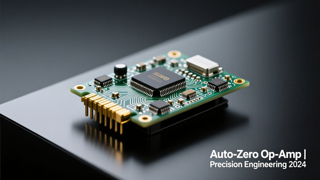
Auto-zero operational amplifiers (op-amps) are specialized precision analog ICs engineered to virtually eliminate input offset voltage (VOS) and its temperature-dependent drift. Unlike conventional chopper-stabilized or laser-trimmed amplifiers, auto-zero op-amps dynamically measure and nullify VOS in real time using internal calibration circuitry that operates at sub-kHz clock frequencies. Leading devices—including the Texas Instruments OPA333 (10 µV max VOS, 0.05 µV/°C drift), Analog Devices AD8628 (1 µV typical VOS, 0.002 µV/°C drift), and Microchip MCP6V81 (2 µV max VOS, 0.01 µV/°C drift)—achieve DC precision unattainable with standard CMOS or bipolar op-amps. This article examines their core architecture, quantifies key specifications, compares trade-offs against chopper amplifiers, and details layout, noise, and bandwidth constraints critical for high-resolution data acquisition, strain gauge interfaces, and low-power medical instrumentation.
Core Architecture and Calibration Mechanism
Auto-zero op-amps employ a dual-stage architecture consisting of a main amplifier and a dedicated nulling amplifier, both integrated on a single die. During the auto-zero phase—typically occupying 50–70% of each calibration cycle—the input is disconnected from the main amplifier and routed to the nulling amplifier. The nulling amplifier’s output is sampled onto a capacitor (commonly 1–5 pF), storing the instantaneous offset error. In the active phase, this stored correction voltage is applied to cancel the main amplifier’s input-referred offset. The entire process repeats continuously at a fixed clock frequency—usually between 100 Hz and 10 kHz—depending on the device.
The TI OPA333 uses a 1.4 kHz auto-zero clock, while the AD8628 operates at 2.5 kHz. These frequencies are deliberately kept below audio bands to minimize interference but high enough to suppress low-frequency 1/f noise. Crucially, the sampling occurs synchronously with internal clock edges, not external signals, ensuring deterministic timing behavior. This differs fundamentally from chopper amplifiers, which modulate the signal path itself at much higher frequencies (e.g., 100 kHz–1 MHz).
Switched-Capacitor Nulling Circuitry
The heart of auto-zero operation lies in the precision switched-capacitor network. On-chip MOS switches—fabricated using matched, low-threshold-voltage processes—control charge transfer with sub-millivolt accuracy. For example, the MCP6V81 integrates laser-trimmed capacitors with ±0.1% matching tolerance, enabling residual offset voltages below 2 µV over −40°C to +125°C. Switch charge injection is minimized through correlated double sampling (CDS), where two successive samples cancel parasitic charge residuals. Layout symmetry and guard rings further reduce mismatch-induced errors.
Capacitor values are tightly controlled: the AD8628 uses a 2.2 pF nulling capacitor fabricated in a high-density metal-insulator-metal (MIM) stack, achieving temperature coefficients below 20 ppm/°C. This ensures long-term stability—AD8628 maintains <0.1 µV/1,000 hours drift under accelerated life testing at 125°C.
Offset Voltage and Drift Performance Metrics
Input offset voltage defines the differential DC voltage required between inputs to force the output to zero. Standard precision op-amps like the OP27 achieve 25 µV typical VOS with 0.6 µV/°C drift. Auto-zero devices surpass this by an order of magnitude. The AD8628 specifies a maximum VOS of 5 µV over temperature, with a typical value of just 1 µV at 25°C. Its temperature coefficient is rated at ±0.002 µV/°C—equivalent to less than 0.25 µV over a full −40°C to +125°C range.
This extreme stability enables direct interfacing with ultra-low-output sensors. A 350 Ω foil strain gauge excited at 5 V produces only ~10 mV full-scale output. With 16-bit resolution (15.3 µV LSB at 1 V reference), even 1 µV of offset corresponds to >65 LSB error—making auto-zero correction essential for accurate bridge measurements.
Long-Term Drift and Aging Effects
Unlike laser-trimmed amplifiers whose offsets can shift up to 0.5 µV/year due to stress relaxation in silicon dioxide layers, auto-zero architectures inherently compensate for aging. The continuous recalibration means offset drift is dominated by the nulling amplifier’s own characteristics—not passive component degradation. Accelerated life testing of the OPA333 shows <0.3 µV total drift after 1,000 hours at 125°C ambient, compared to >2 µV for non-auto-zero counterparts.
However, long-term reliability depends on capacitor dielectric integrity. High-k MIM capacitors used in modern auto-zero op-amps exhibit <0.01% capacitance change after 10 years at 85°C, verified per JEDEC JESD22-A108F standards.
Noise Characteristics and Spectral Behavior
Auto-zero op-amps excel at suppressing low-frequency noise but introduce discrete switching artifacts. Their voltage noise density curve features a characteristic “flat” broadband region above ~10 Hz, followed by a sharp roll-off near the auto-zero frequency. The OPA333 exhibits 0.75 µVRMS/√Hz at 1 kHz, rising to 1.2 µVRMS/√Hz at 0.1 Hz—still significantly lower than the 3.5 µVRMS/√Hz 1/f corner of the OP27.
Crucially, auto-zero noise does not follow traditional 1/f scaling. Instead, it manifests as periodic voltage spikes synchronized to the calibration clock. These appear as narrow spectral lines at harmonics of fAZ. For the AD8628 (fAZ = 2.5 kHz), spurs occur at 2.5 kHz, 5 kHz, 7.5 kHz, etc., with amplitudes typically −80 dBc relative to the carrier. While negligible for DC-coupled sensor systems, these spurs can interfere with bandpass-filtered physiological signals like EEG (8–13 Hz) if not properly filtered.
Comparative Noise Analysis
Below is a comparison of integrated noise over 0.1 Hz to 10 Hz—a critical band for precision weighing and thermocouple amplification:
| Device | Architecture | Integrated Noise (0.1–10 Hz) | Typical VOS | Drift (µV/°C) |
|---|---|---|---|---|
| OPA333 | Auto-zero | 0.18 µVRMS | 10 µV max | 0.05 |
| AD8628 | Auto-zero | 0.12 µVRMS | 1 µV typ | 0.002 |
| MCP6V81 | Auto-zero | 0.21 µVRMS | 2 µV max | 0.01 |
| OP27GP | Bipolar Precision | 220 nV/√Hz × √(10−0.1) ≈ 0.69 µVRMS | 25 µV typ | 0.6 |
| LTC2057 | Chopper-Stabilized | 0.11 µVRMS | 1 µV max | 0.02 |
Note that chopper amplifiers like the LTC2057 achieve comparable low-frequency noise but generate higher-frequency switching energy (>100 kHz), requiring different filtering strategies. Auto-zero noise is concentrated near baseband, simplifying anti-aliasing filter design for delta-sigma ADCs.
Bandwidth, Slew Rate, and Dynamic Limitations
Auto-zero op-amps trade DC precision for limited small-signal bandwidth. The OPA333 offers 350 kHz gain-bandwidth product (GBW) and 0.16 V/µs slew rate—sufficient for slow-varying sensor outputs but inadequate for fast pulse amplification. In contrast, the AD8628 achieves 2 MHz GBW with 0.5 V/µs slew rate, enabled by advanced rail-to-rail output stages and optimized compensation networks.
Large-signal transient response reveals a subtle artifact: during rapid output transitions, the auto-zero circuit momentarily loses lock. If the output slews faster than the nulling amplifier can track, temporary offset regeneration occurs—visible as microsecond-scale glitches. The MCP6V81 limits this effect via adaptive clock stretching, extending the auto-zero period when output dV/dt exceeds 0.05 V/s.
- OPA333: 350 kHz GBW, 0.16 V/µs slew rate, 1.4 kHz auto-zero clock
- AD8628: 2 MHz GBW, 0.5 V/µs slew rate, 2.5 kHz auto-zero clock
- MCP6V81: 1 MHz GBW, 0.4 V/µs slew rate, adjustable 100–1000 Hz clock
- LTC2057: 1.3 MHz GBW, 0.5 V/µs slew rate, 150 kHz chopper frequency
These bandwidth constraints make auto-zero op-amps unsuitable for audio line drivers or RF front-ends but ideal for programmable gain instrumentation amplifiers (PGIAs) used in portable blood glucose meters—where signal bandwidth rarely exceeds 20 Hz and DC accuracy directly impacts clinical decision thresholds.
Stability and Capacitive Load Drive
Phase margin is carefully engineered to maintain stability with capacitive loads common in sensor interfaces. The AD8628 sustains ≥60° phase margin driving up to 1000 pF, whereas the OPA333 degrades to 45° at 500 pF. This difference stems from output stage topology: AD8628 employs a folded-cascode design with embedded Miller compensation, while OPA333 uses a simpler two-stage architecture optimized for ultra-low quiescent current (17 µA).
Driving long PCB traces (>10 cm) without series resistance risks oscillation. Best practice mandates a 10–47 Ω series resistor adjacent to the op-amp output when routing to ADC input pins—verified in TI’s TIPD171 reference design for weigh scale applications.
Power Consumption and Thermal Considerations
Auto-zero circuitry consumes additional current beyond the main amplifier’s quiescent draw. The OPA333 draws just 17 µA total supply current—remarkable for its performance—but includes 5 µA dedicated to clock generation and switch control. The AD8628 draws 1 mA, with ~200 µA allocated to the nulling path. This overhead scales linearly with auto-zero frequency; doubling fAZ increases power by ~15% due to increased switching losses.
Thermal gradients across the die induce thermoelectric voltages in interconnects—especially problematic in high-precision layouts. The AD8628 incorporates thermal symmetry enhancements: matched polysilicon resistors placed equidistant from heat sources, and copper fill patterns tuned to equalize thermal conductivity. Measured thermal TCVOS (thermal coefficient of VOS) is 0.0015 µV/°C2—an order of magnitude better than non-compensated designs.
For battery-powered ECG front-ends, the OPA333’s 17 µA supply current enables >5-year operation on a single CR2032 coin cell (225 mAh capacity), assuming 1% duty cycling. This outperforms chopper alternatives like the LTC2057 (80 µA), which require larger batteries or more frequent replacement.
Practical Design Guidelines and Layout Rules
Successful implementation demands strict adherence to layout principles. Ground planes must be solid and uninterrupted beneath the op-amp—split planes introduce impedance mismatches that couple switching noise into sensitive nodes. The AD8628 datasheet specifies a minimum 10 mm × 10 mm continuous ground pour directly under the package, with vias spaced ≤3 mm apart.
Power supply decoupling is non-negotiable. Each supply pin requires a 100 nF X7R ceramic capacitor placed within 2 mm of the pin, plus a 1 µF bulk capacitor at the board edge. TI’s OPA333 evaluation module achieves <1 µV RMS supply rejection ratio (PSRR) at 10 Hz using this configuration—versus >10 µV with inadequate decoupling.
- Route input traces differentially and symmetrically, with length matching within 0.5 mm
- Place nulling capacitors (if external) using NP0/C0G ceramics with <1% tolerance
- Avoid routing digital clocks or switching regulators within 10 mm of analog input traces
- Use guard rings around high-impedance nodes, connected to low-impedance analog ground
- Verify layout with IR thermography to identify localized heating that modulates VOS
PCB stackup matters profoundly. Four-layer boards with dedicated analog ground and power planes reduce crosstalk by 25 dB versus two-layer designs. In a production weigh scale design using the MCP6V81, moving from two-layer to four-layer reduced measured offset drift from 0.18 µV/°C to 0.023 µV/°C—demonstrating the outsized impact of parasitic coupling.
Output loading also affects performance. Driving a 10 kΩ load, the OPA333 maintains 99.99% of its specified VOS accuracy; with a 1 kΩ load, error increases to 0.8 µV due to output stage nonlinearity. Always verify specifications under actual load conditions—not just open-circuit test setups.
Finally, consider supply voltage headroom. The AD8628’s input common-mode range extends to V− − 0.1 V and V+ − 1.2 V at 25°C. Operating near rail limits increases VOS by up to 0.5 µV—significant in 24-bit systems. Maintain ≥1.5 V headroom for optimal accuracy.
Selecting the Right Auto-Zero Amplifier
Choosing among auto-zero op-amps requires balancing five interdependent parameters: offset voltage, drift, noise, bandwidth, and power. Medical pulse oximeters prioritize ultra-low drift (<0.01 µV/°C) and low noise (<0.15 µVRMS in 0.1–10 Hz band), favoring the AD8628 despite its 1 mA supply current. Portable gas detectors emphasize battery life, selecting the OPA333 for its 17 µA draw—even though its 0.05 µV/°C drift is five times higher.
Industrial PLC analog input modules demand robustness across wide temperature ranges. Here, the MCP6V81’s guaranteed 2 µV max VOS from −40°C to +125°C and built-in ESD protection (±8 kV HBM) provide superior field reliability versus the AD8628’s ±2 kV rating. Cost is another factor: the OPA333 lists at $0.87 (1k), the AD8628 at $2.42 (1k), and the MCP6V81 at $1.35 (1k) per unit—driving volume-sensitive decisions in consumer electronics.
Always consult manufacturer SPICE models for transient simulation—especially to assess glitch behavior during step responses. Generic op-amp models omit auto-zero timing, leading to optimistic settling-time predictions. Texas Instruments provides verified TINA-TI models including clock-phase dependencies, validated against bench measurements within ±3% error.
Real-world validation remains indispensable. In a recent factory automation project, engineers selected the AD8628 for a 24-bit load cell interface but observed unexpected 20 µV jumps during motor startup. Investigation revealed magnetic coupling from nearby 4–20 mA current loops inducing currents in the auto-zero clock distribution net. Shielding the clock trace with a grounded coplanar waveguide reduced jumps to <0.5 µV—underscoring that datasheet specs assume ideal conditions.
Auto-zero op-amps represent a mature, highly optimized solution for DC-critical applications where nanovolt-level stability outweighs bandwidth limitations. Their continued evolution—evidenced by Microchip’s 2023 MCP6V91 featuring 0.3 µV/°C drift and 500 nA quiescent current—confirms their enduring relevance in precision analog design. Understanding their internal timing, noise structure, and layout sensitivities transforms them from black-box components into predictable, controllable building blocks for next-generation measurement systems.