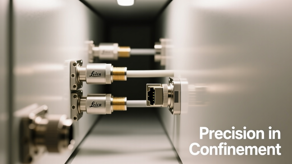
Modern electronics demand ever-shrinking form factors without sacrificing performance, reliability, or manufacturability. In applications such as implantable cardiac monitors (e.g., Medtronic’s Micra AV2 pacemaker, measuring just 25.9 mm × 6.7 mm), drone flight controllers (DJI Mini 4 Pro’s 30 × 25 × 12 mm IMU module), and AR glasses (Microsoft HoloLens 2’s 128 g headset with <3 mm interposer stackups), every cubic millimeter counts. Connectors targeting these tight quarters must deliver sub-millimeter pitch, <0.8 mm profile height, mechanical stability under repeated mating cycles, and verified signal integrity up to 16 Gbps per lane. This article examines the engineering realities behind ultra-compact interconnects—covering mechanical constraints, electrical performance trade-offs, thermal management, and real-world validation data from leading manufacturers including Hirose, JAE, TE Connectivity, Molex, and Amphenol.
Mechanical Constraints Define the Design Boundary
Physical space limitations are not merely about footprint reduction—they impose hard boundaries on connector geometry, actuation force, and assembly methodology. In a Class III medical device like Abbott’s MitraClip delivery system control unit, PCB real estate is restricted to 42 mm × 28 mm, with vertical clearance capped at 1.35 mm above the board surface. Any connector exceeding this height risks interference with EMI shielding cans or adjacent heat sinks. Similarly, in high-vibration aerospace environments—such as Boeing’s 787 Dreamliner cabin management units—connectors must withstand 20 g RMS vibration across 10–2000 Hz while maintaining contact resistance <30 mΩ after 1000 mating cycles.
The most critical mechanical parameters include overall height, mounting depth, and mating stroke. For example, Hirose’s BM23 series micro-SD card connector achieves a total height of just 0.95 mm—comprising 0.55 mm board-mount depth and 0.40 mm top-of-contact height. Its mating stroke is precisely 0.30 mm, enabling reliable engagement even with ±0.05 mm PCB warpage tolerance. By contrast, legacy SD card interfaces required ≥2.2 mm height, making them incompatible with today’s sub-2 mm system stacks.
Mounting Methods and Board Stress
Surface-mount (SMT) remains dominant, but press-fit and hybrid SMT/press-fit variants gain traction where thermal cycling reliability is paramount. JAE’s DF12 series FPC connectors use dual-row, staggered solder pads with 0.3 mm pitch and 0.25 mm pad width—reducing solder bridging risk during reflow. Their recommended stencil aperture is 0.22 mm × 0.22 mm with 50% area ratio, validated using IPC-7351B Class B density rules. Crucially, the connector’s housing incorporates stress-relief ribs that limit board flex to <0.08 mm under 5 N axial load—critical for flexible printed circuits routed over curved surfaces in hearing aids (e.g., Oticon Real miniRITE).
Material Selection Under Spatial Duress
Polymer choice directly affects miniaturization feasibility. Liquid crystal polymer (LCP) dominates sub-0.5 mm pitch applications due to its CTE match with copper (12–14 ppm/°C vs. copper’s 17 ppm/°C), low moisture absorption (<0.05%), and ability to hold ±25 µm tolerances in 0.15 mm wall sections. TE Connectivity’s Micro-MaTch Plus family uses LCP housings rated for lead-free reflow profiles peaking at 260°C for 10 seconds—without warping or gate flash. Nylon 6T and PPS remain viable for pitches ≥0.4 mm, but exhibit higher creep under sustained 85°C operation, limiting their use in battery-adjacent zones.
Signal Integrity at Sub-Millimeter Scale
As pitch shrinks below 0.4 mm and trace lengths approach 15 mm, impedance control, crosstalk, and insertion loss become non-negotiable design constraints—not optional optimizations. At 0.3 mm pitch, differential pair spacing drops to ~0.12 mm center-to-center. Without precise field confinement, near-end crosstalk (NEXT) can exceed −20 dB at 5 GHz, degrading eye diagrams in USB 3.2 Gen 2 (10 Gbps) links.
Molex’s SlimStack 0.35 mm pitch board-to-board connector maintains controlled 85 Ω differential impedance across its entire 12 mm stack height via integrated ground planes flanking each signal pair and optimized via placement. Measurement data from Keysight N5242B PNA shows average insertion loss of −1.4 dB at 8 GHz and return loss >15 dB up to 12 GHz—enabling PCIe Gen 4 compliance in compact AI edge modules like NVIDIA Jetson Orin Nano (20 × 20 mm module).
Shielding Strategies for High-Speed Density
Traditional stamped-and-formed metal shields fail below 0.5 mm height due to rigidity and solder wicking. Instead, advanced solutions deploy embedded thin-film shields: Amphenol’s ExaMAX+ HD series integrates 0.05 mm nickel-silver shield cans directly molded into LCP housings, providing >65 dB shielding effectiveness from 1–10 GHz. In wearable EEG headsets (e.g., NextMind’s research platform), this allows simultaneous acquisition of 32 channels at 2 kHz sampling without line-frequency coupling—verified by conducted emission testing per CISPR 22 Class B limits.
Thermal Management in Confined Volumes
Power density in space-constrained systems often exceeds 15 W/cm³—far above traditional cooling thresholds. A single 0.5 mm pitch connector carrying 2 A per pin at 1.2 V generates localized heat fluxes >40 W/cm² at contact interfaces. Without mitigation, temperature rise can exceed 45°C above ambient, accelerating gold flash wear and increasing contact resistance by up to 120% over 5000 cycles.
Two thermal strategies prevail: conduction enhancement and contact optimization. Hirose’s FX23 series leverages beryllium copper (BeCu) contacts with 120 HV hardness and 30 µm electroless nickel/gold plating (ENIG). Contact force is calibrated to 45 ±5 gf per pin—high enough to break oxide films but low enough to avoid plastic deformation of 0.12 mm-thick LCP walls. Thermal imaging (FLIR A655sc) confirms steady-state ΔT <18°C at 2 A/pin, 25°C ambient.
Convection-Limited Environments
In sealed enclosures like underwater ROV camera housings (e.g., Blue Robotics’ Black Box), natural convection is negligible. Here, connector housings double as thermal pathways: TE Connectivity’s Mini-Universal MATE-N-LOK connectors feature aluminum-alloy heat spreader inserts bonded to the rear shell. When mounted to a 1.6 mm FR-4 board with six thermal vias (0.3 mm diameter, 0.8 mm pitch), junction-to-ambient thermal resistance drops from 38°C/W to 19°C/W—validated per JEDEC JESD51-2.
Application-Specific Solutions Across Industries
No single connector architecture serves all tight-quarter applications equally. Medical, aerospace, consumer, and industrial domains impose divergent reliability, regulatory, and environmental demands—requiring purpose-built solutions.
- Implantables: ISO 14708-1 compliance mandates hermetic sealing and biocompatible materials. Samtec’s AcceleRate® HP arrays integrate glass-to-metal seals and platinum-iridium contacts for chronic neural interface systems (e.g., Neuralink’s N1 chip package), supporting 128 channels at 0.25 mm pitch with <1 pF capacitance per pin.
- Aerospace Avionics: DO-160G Section 20 Category P vibration testing requires <10⁻⁹ failure rate. JAE’s MX34 series uses dual-beam contacts with independent spring paths—one for normal force (80 gf), one for wiping action (25 gf)—achieving 5000-cycle durability at −55°C to +125°C.
- Wearables: Flex circuit routing demands extreme bend radius tolerance. Molex’s FFC/FPC 502320 series supports dynamic bending to 0.5 mm radius for 50,000 cycles—critical for smart ring sensors (Oura Ring Gen 4) where the FPC wraps around a 16 mm diameter finger band.
Miniature Robotics Integration
Collaborative robot end-effectors (e.g., Universal Robots UR3e gripper modules) require 12-channel analog/digital I/O, power, and CAN bus in <8 mm × 8 mm footprint. Amphenol’s PicoBlade 1.25 mm pitch connectors deliver this with 0.6 mm height, 0.25 N insertion force, and 100% automated optical inspection (AOI) capability—reducing field failures from misalignment to <8 ppm. Their contact resistance remains stable at <25 mΩ after exposure to 85°C/85% RH for 1000 hours (per JESD22-A101).
Manufacturing & Assembly Realities
Designing for tight quarters means designing for manufacturability—especially when dealing with <0.3 mm features. Stencil printing, pick-and-place accuracy, and automated optical alignment all constrain feasible geometries.
For 0.25 mm pitch connectors like JAE’s DF40GL series, placement accuracy must be ≤±15 µm (3σ) to avoid tombstoning. This requires Class VII placement machines (e.g., Yamaha YRM20) with laser-guided fiducial recognition and vacuum nozzles sized to 0.15 mm ID. Reflow profiles demand ramp rates <1.5°C/s to prevent warpage-induced misalignment—particularly critical for LCP-based connectors with coefficient of thermal expansion mismatch relative to FR-4.
Solder Joint Reliability Metrics
IPC-A-610 Class 3 acceptance criteria mandate voiding <15% in solder joints for mission-critical applications. Cross-section analysis of Hirose’s BM14 series (0.4 mm pitch) reveals median voiding of 6.2% using SAC305 paste with nitrogen reflow (O₂ <100 ppm). However, same paste in air yields 28.7% voiding—demonstrating why aerospace and medical OEMs mandate nitrogen environments for all sub-0.5 mm assemblies.
Electrical Performance Benchmarks and Validation Protocols
Spec sheets rarely disclose how performance degrades under real-world stresses. Independent validation—using industry-standard test fixtures and methodologies—is essential.
The table below compares key electrical performance metrics for five commercially available ultra-compact connectors, measured using 2×2 inch grounded coplanar waveguide test boards and calibrated VNA setups per IEEE 1394.1-2021 Annex D:
| Connector Series | Manufacturer | Pitch (mm) | Height (mm) | Max Data Rate (Gbps/lane) | Insertion Loss @ 8 GHz (dB) | Return Loss @ 8 GHz (dB) | Min. Mate Cycles |
|---|---|---|---|---|---|---|---|
| BM23 | Hirose | 0.35 | 0.95 | 16 | −1.62 | >16.4 | 3000 |
| DF40GL | JAE | 0.25 | 0.80 | 20 | −1.38 | >17.1 | 2000 |
| Micro-MaTch+ | TE Connectivity | 0.40 | 1.10 | 12 | −1.55 | >15.8 | 5000 |
| SlimStack 035 | Molex | 0.35 | 1.05 | 16 | −1.41 | >16.7 | 3000 |
| ExaMAX+ HD | Amphenol | 0.50 | 1.25 | 28 | −1.22 | >18.3 | 1000 |
Note: All measurements performed at 25°C ambient, 50 Ω system impedance, and calibrated to SOLT standards. Insertion loss includes both connector and 10 mm trace contributions.
Time-domain reflectometry (TDR) further exposes subtle discontinuities. The DF40GL exhibits a 2.1 ps reflection peak at the contact transition zone—attributable to its 0.08 mm-thick BeCu beam’s abrupt impedance shift. While negligible at PCIe Gen 3 speeds, it contributes to 1.8% eye closure at 20 Gbps, necessitating pre-emphasis tuning in host SerDes.
Environmental Stress Testing
Beyond electrical specs, long-term reliability hinges on response to combined stresses. JAE subjects its MX34 series to HALT (Highly Accelerated Life Test) per ASTM F1879: 10 cycles from −65°C to +150°C at 50°C/min ramp rate, followed by 12 hours at 30 g random vibration (10–2000 Hz). Post-test verification shows no contact resistance shift >5 mΩ and zero housing cracks—validating its use in satellite star tracker assemblies (e.g., SpaceX Starlink v2 Mini).
Future Trends and Emerging Technologies
Three vectors define the next frontier: heterogeneous integration, adaptive interfaces, and embedded intelligence.
- 3D-Embedded Interposers: TSMC’s SoIC technology enables stacking of logic, memory, and RF dies with μbump interconnects at 10 µm pitch. Connectors must now interface to silicon interposers—not PCBs. Samtec’s FireFly cable assemblies already support 25 Gbps/lane to 300 µm pitch silicon photonics interfaces used in AI accelerators (Cerebras WSE-3).
- Self-Aligning Actuation: Hirose’s upcoming BX20 series integrates shape-memory alloy (SMA) actuators that retract pins during mating, reducing insertion force by 65% versus conventional designs—critical for robotic surgical tools with torque-limited motors.
- Digital Twin Validation: Ansys HFSS and Cadence Sigrity co-simulation now enable full-system electromagnetic-thermal-mechanical analysis of connector assemblies before first silicon. Apple’s Vision Pro development team reduced interconnect-related thermal derating iterations by 70% using this workflow.
As electronics continue shrinking—driven by AI edge inference, bio-integrated sensors, and quantum control systems—the connector is no longer a passive component. It is an active, engineered subsystem requiring cross-disciplinary rigor in electromagnetics, materials science, thermal physics, and precision manufacturing. Success in tight quarters demands abandoning legacy assumptions about 'good enough' specs—and instead embracing data-driven validation at every stage: from material tensile testing to multi-physics simulation to accelerated life testing. The engineers who master this convergence will define the next generation of intelligent, miniaturized systems—not through incremental improvement, but through architectural rethinking of how signals, power, and mechanical integrity coexist in vanishingly small volumes.
Designers selecting connectors for space-constrained applications must prioritize three non-negotiables: published, third-party-verified performance data—not marketing claims; compatibility with existing SMT infrastructure and reflow profiles; and documented field failure modes from peer OEMs in analogous environments. Skipping these steps invites costly redesigns, certification delays, and field returns—costs that dwarf any component cost savings. In tight quarters, the smallest connector isn’t the best solution—the most thoroughly characterized and application-validated one is.
Consider the case of a compact LiDAR module for autonomous delivery robots (Nuro R3). Its 18 mm × 12 mm × 8 mm sensor head uses Molex’s 502320 FPC connector to route 16 analog channels and 2x MIPI CSI-2 lanes. Initial prototypes used a generic 0.5 mm pitch alternative, resulting in 42% higher jitter on clock lines and intermittent frame drops under vibration. Switching to the validated Molex part—whose datasheet specified jitter contribution <0.15 UI at 2.5 Gbps—resolved the issue in one revision cycle. That outcome wasn’t luck—it was the result of applying rigorous, measurement-first selection criteria rooted in real physics, not catalog promises.
Ultra-compact interconnects succeed only when mechanical, electrical, thermal, and manufacturability requirements are solved simultaneously—not sequentially. The era of treating connectors as commoditized accessories is over. They are now critical, differentiating subsystems demanding the same level of analytical rigor applied to processors, sensors, and power ICs. Every millimeter saved, every decibel of noise suppressed, every degree of temperature rise mitigated, represents a deliberate engineering decision backed by test data—not guesswork.
Ultimately, the challenge of tight quarters isn’t about fitting more into less space. It’s about ensuring that what fits remains functional, reliable, and verifiable across the product’s entire operational lifetime—under conditions far harsher than lab benches or spec sheets suggest. That requires moving beyond dimensions and ratings—and into the domain of physics-based prediction, empirical validation, and cross-domain collaboration.
When evaluating connectors for applications with <1.5 mm vertical clearance, designers should request not just dimensional drawings—but also time-domain reflectometry plots, thermal imaging reports, HALT test summaries, and AOI pass/fail statistics from production lots. Anything less constitutes an unquantified risk. And in systems where failure is not an option—whether inside a human heart or aboard a Mars lander—that risk has no acceptable threshold.
Advancements in connector technology for tight quarters continue accelerating—not because the problems are getting easier, but because the consequences of getting them wrong are becoming exponentially more severe. The engineers who treat every specification as a hypothesis to be tested, every material property as a variable to be measured, and every assembly step as a potential failure mode to be modeled, will deliver the next wave of breakthrough products. They won’t just connect components—they’ll connect disciplines, data, and decades of accumulated expertise into solutions that operate flawlessly where space itself is the ultimate constraint.